Most people who use a PCB autorouter switch it off within an hour. It finishes the easy nets, makes a mess of the hard ones, and leaves a board no engineer would sign. We set out to build one that a designer could trust, inside Open PCB & IC Engineer, our free, open-source design tool. This is the story of that work so far: what we built, what went wrong, and what each mistake taught us.
It is written for new engineers, and it keeps the mistakes in on purpose. Each one cost hours or days, and each one left a lesson behind, along with the numbers that proved it. Arthur put it plainly when we began collecting them: say that we are not perfect. That is part of why PCBICEng is open source under the GPL v3. Anyone can see where it falls short and help make it better, and the mistakes listed here are good places to start.
Table of Contents
The Rules We Set Before Routing A Single Net
Before writing a router, we decided how we would know whether it worked. Three rules came out of that, and they saved us many times.
Pick a judge you did not write. Every result is checked by KiCad‘s own design-rules check (DRC), the same check a designer runs before sending a board to the factory. We did write our own checker, because the router needs one inside its loop, but we trusted it only after it agreed with KiCad’s counts on six demonstration boards. Pours have to be refilled before judging, too. A pour stored in the file from before routing shows copper where new tracks now run, and it reports errors that are not there while it hides some that are.
Test your assumptions against the reference, not against your reasoning. Our first guess was that KiCad joins two pieces of the same net only where their ends meet. KiCad’s DRC showed otherwise: any overlap connects, crossing tracks included. A short test on the real judge settled what an hour of reasoning could not.
Round-trip before you route. The first milestone wrote each board’s own tracks back out through our writer and checked that KiCad saw the same board. A router whose output cannot be read back cleanly proves nothing. That rule caught a serious bug weeks later, when boards with added layers came out unreadable, and we will come back to it.
A First Engine, And A First Humbling
The engine is a classic design. The board becomes a grid of cells, a fraction of the smallest clearance across, on every copper layer. A search called A* finds each connection’s path, moving in 45-degree steps and changing layers by vias. Then a method called PathFinder settles the arguments. At first, nets may share cells. Every round, the shared cells become more expensive, until each net finds a place of its own. Spacing is kept by “halos”: each net’s copper marks the cells another net’s track centre may not use.
Four stripped two-layer KiCad demonstration boards were rerouted with no clearance errors and no shorts by KiCad’s DRC. KiCad’s own hand-routed mixer board has twelve. That felt like a good start.
Then we were asked to make the search smarter, and we built two well-known ideas. The first was global planning: route every net first on a coarse grid of tiles, then keep the detailed search near that corridor. The second was blocker-aware rip-up: when a net is stuck, remove the nets in its way and route it first.
On a 108-net, four-layer board called tinytapeout, after 100 rounds, the plain router ended with 2 nets in conflict. With rip-up it ended with 6. With planning and rip-up together it ended with 10, and planning alone left 6. Neither idea helped.
An idea that is “obviously smarter” must win on measurements. Keep the experiment, publish the numbers, and move on.
Both ideas are still in the code, switched off, with their numbers beside them, so the next engineer does not try them again blind.
Read The Board Before You Search Harder
RoyalBlue54L, an eight-layer board, routed only 20 of its 68 nets. Instead of tuning the search, we read the board and compared it with what its human designer had done. Three things were wrong, and none of them was the search.
- All six inner layers were treated as solid planes. The designer had routed signals on three of them. Those were split planes, power layers that carry a few tracks. Now a net with several plane layers keeps its largest as a plane, and its other layers can be routed at a cost.
- The net classes said 0.25 mm tracks and 0.8 mm vias, but the designer used 0.15 and 0.45 mm where the board was tight. The project file lists those preset sizes. Now a net stuck for ten rounds steps down the presets, never below the board’s minimum and never for a differential pair, and the report names every net it narrowed.
- Drilled holes came too close together. Our grid did not know about hole-to-hole spacing at all.
With those three fixed, all 68 of 68 nets routed, and KiCad’s DRC matched the original board’s.
When a router fails on a real board, the first question is not “how do we search harder?” It is “what does this board’s designer know that our model does not?” Even the trigger for narrowing mattered: stepping down after six rounds narrowed 57 nets and still left two conflicts, and after ten rounds it narrowed 40 nets and left none. Nets that the negotiation would have sorted out on its own had been narrowed too early.
A Net Tie, Read Three Times
A net tie joins two nets on purpose, such as two grounds joined at one point. Our first rule was that tied nets may come close to each other’s copper. KiCad flagged a track 0.09 mm from a tie’s pad. KiCad’s real rule is narrower: only the tie’s own pads may touch, and a track of one net passing the other net’s pad keeps full clearance.
The fix had a bug of its own, found the next morning. Overnight, both test boards got worse, one with two shorts. To let a tied pad’s own net reach it, we had let it use grid cells marked “blocked”. But some of those cells were blocked by a different pad nearby, so vias landed on other nets’ pads. Then came a third problem: a via’s drilled hole sat too close to the tie’s copper bridge. A hole keeps the hole clearance from copper even when the copper belongs to its own net.
When the tie was finally right, RoyalBlue54L routed 68 of 68 in 110 seconds and tinytapeout 108 of 108 in 274 seconds, the first time it ever finished. Two lessons: a fix is a change too, so rerun everything after it, on every board. And “blocked” is not one thing. A cell blocked by your neighbour and a cell blocked by a stranger must be told apart.
Grids Are Round, Copper Is Not
A grid keeps spacing in whole cells, so two tracks can end up a few micrometres closer than the rule allows. So after the grid, an exact pass moves track corners and vias apart, by at most three quarters of a cell, and necks short pad entries down to the board’s minimum width. A net counts as done only when it passes the exact check. Usually that pass turns 15 to 46 too-close pairs into none.
The gap between the grid and the real geometry came back again and again. It was the most persistent problem of the whole project, so it is worth following through:
- The diagonal off by a hair. When we tried routing a differential pair as one object, the partner’s offset of four cells on a diagonal is 5.66 cells long, and the spacing marks reached 5.72. Every diagonal stretch showed the pair in conflict with itself. When two parts of a program each round to the grid, they must round the same way.
- The corner rule. A diagonal step was allowed only when both cells beside it were free. A designer’s 45-degree track squeezed between two others leaves a band one cell wide, whose side cells are always taken, so every diagonal step along it was refused. Arthur agreed: “yes, that rule is mistaken.” With it and a small safety margin turned off, the exact check found no new clearance issue on any of 371 nets of a video board. The rule had been blocking legal paths, not preventing illegal ones. Turning off a safety rule is safe when there is a check after it.
- A gap no cell was on. On OrangeCrab, an open-source FPGA board with a 0.5 mm-pitch BGA, the way out for RAM_D0 is a 0.089 mm track between two balls 0.27 mm apart. A track and its two clearances need 0.267 mm, so the track’s centre has 1.5 micrometres of freedom either side of one exact line. Our grid cells sat 20 micrometres either side of that line, and both were blocked. A BGA sits on its own drawing lattice even when the rest of the board does not, and the closer look now aligns its grid to the lattice of the pads around it.
- A gap 2 micrometres too narrow. The most recent case was the opposite. Two nets on OrangeCrab missed their clearance by about 2 micrometres in every pass. A power via stood 0.424 mm from a locked 45-degree jog of another net, and a track needs 0.426 mm to pass between them. No route could ever fit, but the grid thought one could. The fix was the one the board’s own designer would make: move the locked jog 10 micrometres. A near-miss of a few micrometres at the same spot in every pass is a closed gap, not a bad path.
Arthur asked once whether cells one micrometre wide would fix all of this. In principle, yes. In practice, the cell count grows with the square: a 100 mm board is a million cells per layer at 0.1 mm and ten billion at one micrometre. Nearly all our misses were under 25 micrometres, in a few tight places. So the answer was to look closer only where stuck. More on that below.
Finished Is Not The Same As Good
Arthur gave the router its most important bias early on:
An experienced designer choosing between 8 and 10 layers for a motherboard would most likely take 10: not because 8 cannot be finished, but for better noise and fewer timing races.
“100 % routed” is not the goal. Margin is. So the router had to learn to judge noise, coupling and timing, not just completion.
A Field Solver You Can Trust
To know a track’s impedance, delay and coupling to its neighbours, the tool solves the electric field in a cross-section of the board. We checked it against formulas whose answers are exact, before using it on anything. The first results were 2.5 to 3.5 % low. Halving the cell size halved the error, so the error was first order, which is what you expect at a thin conductor’s sharp edge. Knowing that, two solves at two cell sizes can be extrapolated to zero size. That brought every result within 0.1 % of the exact answers.
Physics gave a second check, better than any number. Two coupled tracks buried in one dielectric must have zero far-end crosstalk, and two on the surface must not. Both held, which showed that the inductance was right as well as the capacitance.
We also learned when a number means nothing. A board with no plane has no defined impedance, because the return current flows wherever the ground tracks go. The report now says so instead of printing 270 ohms. One of us also assumed a 0.2 mm track over 0.2 mm of FR4 should be “about 50 ohms” and suspected a bug at 67. The formulas agreed with the solver: 50 ohms needs a track about twice as wide as the dielectric is thick. Check your intuition before calling it a bug.
Return Paths, And Three False Alarms
A signal’s current comes back through the plane right under its track. Where the plane has a gap, the return goes around, and the loop it makes radiates, picks up noise and changes the line’s impedance. Our check samples every signal track every 0.1 mm against its reference planes.
The first run raised three false alarms, and each one taught something. Every “gap” was exactly 1 mm long, at connector rows: a track entering its own through-hole pad crosses that pin’s clearance hole in every plane, which is unavoidable. A supply with a prefix in its name was taken for a signal. A signal’s own pour was counted as a reference plane. With those fixed, the real finding appeared: on tinytapeout, our router ran 129 mm of track over gaps where the human ran 21 mm, because it routed signals through a split power plane.
Adding a cost for return paths taught us something about pushing one number hard. A high return cost halved the gaps but put crosstalk at 8 % and took fifteen minutes. Making the split plane more expensive everywhere did better on both counts, and faster. The cheapest fix was the habit every designer already has: stay off the plane layers unless you must.
Budgets: A Number Is Not A Verdict
“Worst noise 2.9 %” means nothing until you know what that net can stand. Budgets turn the reports into a pass or a fail per net. A file beside the board sets each net’s edge rate, noise budget, timing skew and switching group.
Groups change what crosstalk means. Nets that switch on the same clock edge, the lines of a bus, couple onto each other during that edge. Nobody samples the line at that moment, so it is not noise, but it moves the edge. On the human’s tinytapeout, grouping three buses took one line from 3.96 % noise to 1.02 %: most of what it heard was its own bus.
The budgets also showed us how to check the checker. On the two-layer demonstration boards, nearly every net failed its gap budget, and so did nearly every net of the human-routed originals: 31 of 31 on one board. On a two-layer board, half the tracks run on the ground layer itself, so the default budget measured the stackup, not the routing. Before you try to beat a number, see whether the human’s board passes it.
A Model Checked The Wrong Way
The router cannot ask KiCad to refill its pours between passes, so it estimates the fill itself. We checked the estimate against KiCad’s own fills by area, and it covered every square millimetre KiCad filled. Yet the noise check against KiCad still disagreed.
The reason was thermal reliefs. KiCad’s ground pour does not touch a ground pad. It leaves a ring crossed by four spokes. A track running 0.34 mm from a ground pin had no copper under it on any layer. The rings are tiny in area, so checking by area hid them, but they sit exactly where tracks run, beside pads. Validate a model by what it is used for, not by a global total.
Then came the opposite error. With reliefs modelled, the estimate found far more gaps than KiCad did, because 149 stitching vias on that board are marked in the file as solidly connected, with no relief at all. Settings on single pads and footprints now come from the file as well.
Stitching, And Measuring What Is Left
A pour that tracks have cut into pieces loses the pieces that no via of its net reaches. KiCad’s refill deletes them as islands, and the layer beside them loses its reference over a whole area.
A designer prevents that with stitching vias, so the router learned to add them: a via of the pour’s net in each island big enough to matter, where it fits clear of every other net on every layer. On tinytapeout it stitched 54 islands, KiCad kept about 300 mm² more ground on each outer layer, and the vias with no return nearby fell from 201 to 161.
But the tracks over gaps did not move at all: 43.8 mm before and after. Those islands were slivers between parallel tracks, too narrow for any via. So we split the 43.8 mm by kind before attacking it again. Only 12.7 mm was over plane our own tracks had cut. The other 31 mm was where no layer has copper at all, around connectors and holes, which the human’s routing crosses too. The part the router could still win was about 13 mm, not 44. Measure the remainder before you attack it.
Eight Layers Or Ten
Arthur’s 8-or-10 judgement became a tool, the layer adviser. It routes the board twice, as it is and with a signal layer and a ground plane added, and compares what the budgets measure. On RoyalBlue54L, going from 8 to 10 layers took the worst noise from 1.7 % to 0.9 %, the vias with no nearby return from 67 to 26, the vias from 291 to 243, and the track from 1520 to 1449 mm. One net went over its gap budget, by 0.15 mm.
The first verdict said “keep 8 layers”, because of that one small loss. One tiny regression had outvoted five large gains. Now the verdict lists the gains and the losses and calls it a trade. An adviser that hides its reasons behind one word gets the bias wrong in both directions.
Pairs And Buses: Order, Not Cost
A differential pair, such as USB’s D+ and D−, must run side by side at a fixed gap and arrive at the same time. Our first attempts made the second net of a pair cheap only along a band beside its partner. At one setting, D− took a 35 mm detour and arrived 99 picoseconds late. The human board is matched to 2.8 ps.
Plots showed why. Other nets’ vias and tracks already sat in the corridor beside D+, the one place D− belongs. They had been routed there in the first rounds, and by the time D− came, the price of crossing another net had grown for 40 rounds, so any detour was cheaper. The cost was never the problem; the order was. A person routes the critical pairs first, while the board is empty.
Now pairs go first, each followed at once by its partner. On RoyalBlue54L, D+ and D− came out 18.6 and 19.4 mm, side by side, 4.9 ps apart. The whole board came out better too, and routing took 178 seconds instead of 307.
On a crowded board, that was not enough. The second net of a pair has exactly one good place, and in the negotiation it kept giving way to nets that had many. A “pair hold” now keeps a pair’s net in place for up to eight rounds, and the others move.
Meanders, Trees And Bundles
Even when they finish, the nets of a pair or a bus arrive at different times. Meanders fix the last part of that: U-shaped bumps added to the faster lines until they arrive together. Their legs stay three track widths apart, because closer bumps couple and shorten themselves electrically. Pair bumps stay low, so the two lines stay coupled.
Meanders trim; they do not plan. tinytapeout’s out bus differed by about 90 mm of routing, and meanders alone only took it from 632 picoseconds of spread to 465, against a 200 ps target. Three steps got it there, each fixing the previous step’s limit:
- Meanders trimmed the small differences.
- Prim–Dijkstra trees, an idea from chip design, stopped bus lines from being built as long chains, where each pin was joined to the nearest pin still open. With the balance set at one half, the out bus went from 465 to 294 ps.
- Bundles routed a bus’s lines one after another in a shared corridor, held loosely, so that lines which kept fighting for room were let go. The out bus reached 134 ps.
For the first time, all five groups on tinytapeout were inside their match.
Good Ideas, Measured And Kept Off
Two more ideas sounded right and lost on the boards. The first was two-sided gap negotiation: a net over a gap made the tracks that cut the gap more expensive too, so both sides would move. On tinytapeout it left 11 nets over budget instead of 8. The cutters moved, made new gaps, and the noise passes chased them.
The second was “room for two”. The first net of a pair paid for every step where its partner could not fit beside it. It was a big win on one board and a loss on the others:
| Board | Skew with the pair hold | With room for two |
|---|---|---|
| tinytapeout | 11 ps | 1.9 ps |
| RoyalBlue54L | 3.3 ps | 36 ps |
| cm5, 18 pairs summed | 206 ps | 356 ps |
The first net went the long way round to find room that the second net, routed separately, then did not take. Leaving room for a partner only pays if the partner is routed into it, and that means both halves in one search. Routing both nets of a pair in one turn broke the negotiation in its own way: the first always went first, so the second always lost. A method that looks right is not better until it beats the old one on the same boards. Both ideas are options, switched off, with these numbers beside them.
One Run Is One Sample
Then a lesson that changed how we measured everything. The router has no randomness, yet its result behaves like a random draw. When two nets want the same cells, whichever is routed first takes them, and a tiny change anywhere can turn one early decision the other way. We nudged one search weight by a few percent and ran each board three times. The spread across those runs was as large as most of the effects we had been reporting. On tinytapeout, the USB pair’s skew ranged from 5 to 172 ps with no change to the code at all.
Worse, a result we had reported did not come back. The committed code, run the next morning, gave 695 ps where the commit message said 130. The router turned out to be deterministic: the reported run had come from a build that differed from what was committed. Run the benchmark from the exact commit before writing its numbers into the commit message, and keep the program with its results. Every results folder now holds a copy of the program that made it.
So the router can now route a board several times at once, with the search weight nudged each time, and keep the best by a fixed score. Completion became reliable: tinytapeout finished every time, against 4 times in 12 for a single try. The quality did not improve, though, because the score put finishing first absolutely and gave up better boards to get there. A score is a decision about what matters most, and it should be made on purpose.
Plan Before You Route
Arthur’s rule as an electrical engineer: know what signals you have and where they need to go before anything else is decided. The router had been doing the opposite. It routed every net the same way and found out afterwards which ones were fast, which belonged together and which were noisy.
So the tool now reads each net the way a designer reads a schematic, from its name, its pins’ names and types, and the parts it joins. The strongest evidence is on the chips, not in the net names: a chip with CLK, CS and IO0 to IO3 pins is a QSPI flash, so its nets are one group, even when one of them is called boot_mode.
The first version made every mistake you might expect from reading names. PWR_EN was taken for a power net, an enable pattern matched GREEN, and nCLKREQ was taken for a clock. Each was found by reading the tool’s own tables, and each rule was then checked on a board it had not been written for.
It also measured something useful about placement. Every place where two nets’ straight-line connections cross has to become a via or a detour, whatever the router does. That count of crossings per connection predicted how hard a board would be to route better than the usual congestion estimates. It ranged from 0.2 crossings per connection on a board that routed in 0.6 seconds to 4 on one that took 22 minutes. An automatic placer that reduced crossings on a Z80 computer board cut the via count from 219 to 121, and the routing time from 41 seconds to 15.
Two Plans That Made Things Worse
Not every plan helped. When we made each net pay more for any layer the plan had not given it, the router used about 20 % more vias, and every via is a break in the return path of its own. The plan picks the right layer for a bus, but a per-cell price is the wrong way to get the bus there.
Planning each bus as one wide trunk did not help either. Holding a bus’s lines together on tinytapeout held them over the same split plane, and the misses went up. The layer plan had already said, before any of those runs, that on that board the noise comes from the stack, not from the routing order. Both ideas are still in the code, switched off.
How Many Layers?
Arthur pushed the thinking in a new direction: “We’re not using the right logic for the autorouting problem… we should be thinking just like Blender!” Treat each trace as an object in 3D, start with plenty of layers and work down to 10 at most, fewer if the noise allows. That is the difference between a maze router like ours and a topological one, which first decides which traces cross and who goes where, and leaves the exact geometry until last.
A first layer predictor colours each board’s crossings onto stacks of 4 to 20 layers in under a second. Routing then checked it on tinytapeout at 4, 6 and 8 layers. At 6 layers the noise was fine, which the prediction had said it would not be. But the QSPI flash bus missed its 50 ps timing match, because there was no room near the chip to lengthen its short lines. Only 8 layers met timing. Arthur decided: “timing counts, go with 8 layers.” Quiet means noise and timing both.
Fifty Ohms, And Half A Dielectric
What width should a bus line be? Arthur’s starting point was the DIP era: 0.1 inch between the legs, so a 0.020 inch trace fits between them with clearance to spare. Modern fine-pitch parts have no room between their pads at all, so a trace necks down there anyway, and on the open board the width is free. Put in impedance terms, he chose “50 ohms per layer”: every signal layer gets the width that makes a 50-ohm line on its own cross-section, because an outer layer over thin prepreg and an inner layer between two planes need different widths.
The first answer was nonsense. On tinytapeout’s outer layers, 50 ohms needed a track narrower than the board’s minimum width. The cause was an old mistake in reading the board. Its stackup lists each outer prepreg as two sub-layers of 0.068 mm, and our reader kept only the first.
So every impedance, delay and coupling the router had worked out for tinytapeout since the field solver was built had been for a board with half its real outer dielectric. With the sub-layers added up, the outer layers came out at 0.215 mm for 49.9 ohms. Earlier results on that board had to be run again.
A File Only Our Own Checker Could Read
The layer tests added copper layers to boards, and the writer put tracks and vias on them. KiCad then reported 199 items “on a disabled layer” and 499 unconnected. The file still listed four copper layers, so KiCad never knew the new ones existed. Our own checker had read the same file as fine, because it took the layers from the router’s list, not from the file.
Writing a board with added layers needs far more than adding names. The inner layers must be renamed into their physical order, the stackup rebuilt with new copper and dielectric entries, every zone, pad and track remapped, and the new planes given zones of their own. Only a check by another program shows what a file really says. That was the round-trip rule from the first week, proved again.
The same rerun showed the USB pair at 108 mm on one line and 51 mm on the other. The pair pass routes a pair’s second net beside its first, but when the first has gone a long way round, following it costs more than going straight, so the second went its own way, on another layer for the whole length. Now, when the first ends up more than 15 % longer, it is routed again beside the second. The pair came out 55 and 51 mm, and after meanders 2.5 ps apart against a 10 ps match.
The Live Board, And What “Instant” Really Takes
Arthur’s next direction was a live board: every part and trace kept in memory, rules that trigger routing as events, so that dragging a chip reroutes its traces at once. A correction came first. The batch router never touched the disk while routing; its ten to twenty minutes were all computation. What makes interactive routers fast is not memory but scope: a change reroutes only the traces it touches.
Arthur also settled the order question that worries everyone about routing one trace at a time: “data and address lines should go first anyway.” The order became a design rule, not a flaw.
The first local router took 43 seconds to reroute three nets, and a second try ran for over 20 minutes. One cause after another came out: a finishing pass that let go of every nearby net, until a local route became a whole-board route; moving a part ripped up all copper of each of its nets, which for ground is the whole board’s ground; and a search window that was small while everything around it still worked on the whole board.
After the fixes, a 0.5 mm move took about a second, or 0.39 seconds once the board’s grid was kept in memory and only the spots that changed were repainted.
One bug from this stage is worth telling, because a tool hid it. Inside a window, the router saw no planes at all. A layer counts as a plane when one pour covers more than 30 % of the board, and the pours had been cut to the window first. Every local route had run without knowing that In1 was ground. Our own test script had filtered the “is a plane” lines out of what it printed.
On the biggest boards, speed became the limit. Four modern boards with 325 to 902 nets were still converging when their hour ran out. Timing each round showed why: 99 % of the time was the search, and each net’s search grew slower every round.
The search’s estimate of the rest of a path stays at the cheapest price, while the negotiation keeps raising real prices, so the search explores everything nearer than the crowd. An estimate that keeps up with the prices finished a 325-net LPDDR4 board in 30 minutes, with a clean DRC. Measure before restructuring. A parallel rewrite would have sped up a search that was wandering.
Seeing Before Searching: Learning From 23 Designers’ Boards
The most useful test we built is called leave-one-out. Take a board a professional finished. Hold every net’s copper where the designer put it, free one net, and route it. The designer’s board proves a legal path exists, so every net that will not route shows something the router sees wrong. We ran it on 23 boards, from small demonstrations to a 902-net FPGA board.
Arthur called the goal “a virtual vision system made exclusively for the AutoRouter”. After four rounds, five things stood out.
Most failures were seeing wrong, not searching wrong. Drill holes at the wrong size, full via pads drawn on layers that have only the hole, copper text drawn as a box per letter, the designer’s DRC waivers ignored, a KiCad 5 board’s rules lost in the upgrade. Each one either built walls that were not there or hid walls that were. Fixing what the router reads raised the scores more than any change to the search did.
The grid is a lens that blurs, so vision needs two levels. Plan coarsely on the grid, aligned to the board’s own drawing lattice, then finish in exact geometry. Slide corners off the grid, thin a track only where it is too close, end a track anywhere in its pad.
Look closer only where stuck. Loosening the grid everywhere cost nets. Used only as a second look at stuck nets, it cost nothing. When the exact check finds a spot, the router now routes that net again with the spot kept out, and then looks again at 10-micrometre cells in a small window around it.
On 66 near-misses, the keep-outs took the legal count from 18 to 35, and the closer look to 46. But a finer eye can only confirm a path that exists. When the coarse plan picked a channel that was closed, looking closer just showed that more clearly.
Context matters as much as the net. The same thinning rule was right with the neighbours held and wrong with them still being routed.
Designers are teachers, not judges. Their boards show habits our rules lacked, such as thinning a track within a few millimetres of a pad. But some of their copper breaks the rules: one designer’s track on tinytapeout is 17.6 micrometres short of its clearance. A designer’s track shows what is possible, not what is legal.
A Working Board Proves A Way Exists
An M.2-to-PCIe adapter board, the same four-lane link a laptop uses for its SSD, routed only 19 of its 28 nets. Arthur’s reasoning was simple: “if there’s no difference in board size between a board that works and the one under construction, if the parts list is identical, then something is wrong with the AutoRouter.” The finished board proves a solution exists. So we took it apart one piece at a time:
| Held as the designer laid it | Ours to route | Result |
|---|---|---|
| nothing | everything | 19 of 28 nets |
| every via | every track | 14 of 28 |
| everything but one pair | that pair | found a path, failed the exact check beside the next pair’s arc |
| power and ground copper | every signal | 27 of 27 in 2.4 minutes |
Two mistakes came out. The grid drew a kept arc as a straight line from end to end, so its bulge looked free to route through. And with the designer’s power copper held, everything routed, so the failure from scratch was where our router put each ground pin’s via at the fine-pitch connector: right in the pairs’ lanes. The designer put them in a column past the end of the pin row, 1.5 mm apart, with each pair passing between two vias.
After three tries the escape planner put its column at 110.19 mm against the designer’s 110.2, and the board routed 28 of 28 in four minutes with 91 vias. The designer used 92. With a working board in hand, hold its copper and free one piece at a time. The piece that will not route is where the router is wrong, and the designer’s copper shows the right answer.
Turning The Search Around
Power nets took minutes where signals took a second, and the counters inside the search showed why. One power net’s 38 searches pushed 19.1 million starting cells and looked at only 2.3 million. Each connection started from the whole tree routed so far, and with the pour counted as part of the tree, the tree was about half a million cells, each pushed with its own distance estimate.
Sorting the cells instead of pushing them was slower still: the cost was the estimate, not the queue. What worked was turning the search around. When the tree is huge, each connection now searches from the open pads to the tree, which costs almost nothing to mark as a target. That is how a designer draws it, from the pad into the pour. Starting cells went from 19.1 million to 0.6 million.
Room: Does Anything Fit Here?
The grid turned out to be wrong in both directions. Too strict, because a cell counts as taken when its centre is too close, so a designer’s track between two lattice points shows as no way through. Too generous, because when the cells are loosened to find those paths, a via site opens where nothing fits. So we built Room, which answers from the board itself: for a cell at the edge of a mark, does this net’s copper fit anywhere across it, at 25 points a quarter cell apart?
Room cost one board seven nets, and the reason is a lesson about sampling. Four nets had routed earlier through a via 5.8 micrometres off its cell’s centre, in a legal window only a few micrometres wide. Room’s points were 16 micrometres apart, stepped right over the window, and closed the cell. Room now searches from its best point in halving steps down to half a micrometre. Sampling a continuous gap is a second grid with the same blindness, only finer.
A Plane Is Not Always One Net
One night’s run on the DDR5 RDIMM tester showed 20 new failures, nearly all DDR5 data lines, every one too close to a via on an inner layer. We had just taught the router to treat a plane layer as closed only where the designer’s pour actually is. But that layer is a split plane holding eight different supplies’ pours, and only the layer’s main net was counted. The other seven pours looked like open board, and the router ran data lines straight across them. When a rule says “the plane”, ask what a plane layer actually holds.
Say Where The Search Stopped
For a long time a failed search said only what it failed to reach: “no way through to a pad, 52 cells”. We read “52 cells” as the region the search could reach and spent time looking for a sealed pocket around the wrong pad. It was the size of the target pad.
A failed search now says how much it saw and where it got nearest: “searched 576 cells, the nearest point on B.Cu, 241 mm short”. That showed at once that the other end of the net was boxed in. A failure message should say where the search stopped, not only what it failed to reach.
The Mistakes That Taught The Most
A few failures from these rounds are worth telling in full.
An upgrade adds rules, it does not only drop them. OrangeCrab routed 69 of 152 nets, and the RAM lines got no vias at all. The board is from KiCad 5, which had no annular-ring or hole-clearance checks. Upgraded, KiCad filled in its modern defaults, and under those, no via fits between the BGA’s balls. KiCad’s own DRC gave the designer’s board 199 errors of each kind. Recovering a board means recovering the absence of a rule too. With that fixed, and two router mistakes about via sizes, OrangeCrab went from 69 to 143 of 152.
Arthur’s guess about power was right. He suspected power nets were slow because their planes were being split to fit a few thin traces between the big filled areas, and that it was “best to figure out how to do those 2 or 3 other traces on a different layer”.
Measured on one board’s 5 V net: opening the extra planes tripled the search, and the route never used them. Planes are now closed by default and opened per net only when a net cannot route otherwise. Along the way the router learned to think of a power net the way a designer does, as a pour that the pads join, with tracks only where the pour does not reach.
A separator inside a field. To free several nets together, we separated their names with “+”. Net names have “+” in them: +3V3, every USB D+. Split, such a name matched nothing, so the net under test was never freed, and it “passed” without being routed. A whole day’s results were void. A separator has to be one the field cannot contain, and a change to the test harness needs the same regression run as a change to the router.
A designer’s rule break. On one board, the only legal way for a net was blocked by the designer’s own via, which broke the board’s hole-clearance rule. Arthur set the policy: a designer’s rule break is “legalized” only if the fab can build it consistently, by its published capabilities, and only at that spot, never worse than the designer’s own. Any use of it is named in the report. When we first built it, the router used the exception on 42 nets that routed legally without it. It is now a last resort, tried only after every strict try fails.
By the end of round 4, 4,885 of 5,106 nets across all 23 boards routed legally with everything else held, about 95.7 %. In that round only one board went backwards, and we found out why: two mistakes in the new code that decides whether copper fits in a cell. By round 14, with the bugs above fixed, the nets still outstanding across all 23 boards had fallen from 193 to 35 in two days.
Under The Big Chips: From Funnel To Fruit Tree
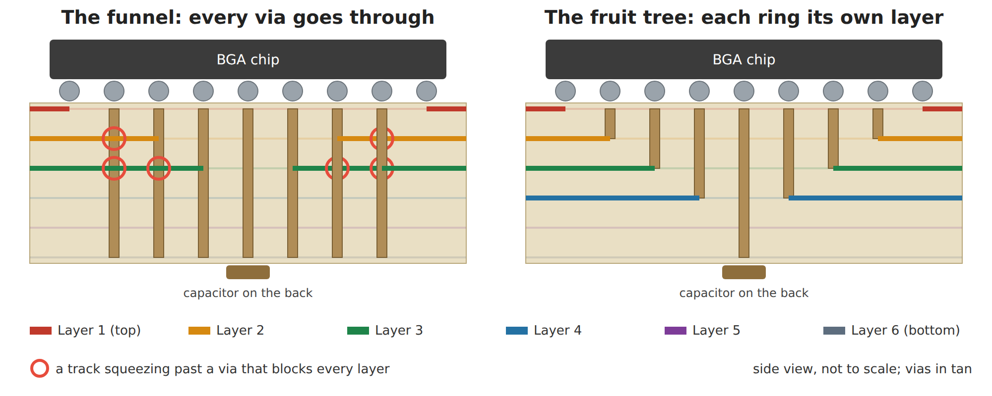
The hardest place on any modern board is under a BGA, where hundreds of balls have to escape past each other. We measured how designers do it on seven arrays from five boards. They drop each signal once, by a single via, straight to its layer, and on the big 1.0 mm-pitch FPGAs nearly all of those vias sit at the diagonal between four balls.
Our first planned escape, a funnel, tangled itself on the hard boards. The idea that worked came from a picture of Arthur’s: a fruit tree, with each ring of balls dropping by a short blind via to its own layer. On a DDR5 test board it routed every net with a clean DRC in a third of the time. That story has its own article.
OrangeCrab: The Board That Kept Teaching
OrangeCrab, a small FPGA board with DDR3 memory, has been the hardest teacher. From scratch, no escape plan finished it. The tree came closest, at 25 % fewer conflicts, which was not an answer.
Every one of OrangeCrab’s problems was on the board before the first track was laid: a ground plane its stackup calls a signal layer, a flash chip right under the FPGA’s bottom row of balls, and a layer too few. Each took days of routing runs to find. So the router now looks before it routes.
In under four seconds it lists every layer as plane, split or signal, where the stackup disagrees with the copper, each ball array’s signals and supplies ring by ring against the room between its balls, and each side’s signals against the room on that side. Its first room model counted every ball site as a via and called two boards that had routed clean “layers short”. Calibrated on three boards, it now agrees with what routing found.
Arthur then drew the FPGA’s escape himself, saying it was “fairly simple to solve, but only for a human”. He assigned layers by their job rather than by ring: the balls’ layer for ground, address and data; one layer for each supply; the bottom for crossovers and the main ground.
He put the supplies on filled vias in their pads, and joined the ground balls to each other across empty sites on the top layer. A count of how much the ball field could carry said all 89 address, data, clock and control lines could leave on the top layer, and a real-geometry escape routed them all in fifteen rounds.
Then we tried stackups by routing each one. Putting the planes first, under the top layer, won clearly: 22 rounds and 3 minutes, against 55 rounds and 26 minutes with the planes at the bottom, where 41 of the board’s 67 capacitors cut a plane to pieces. The chosen stack, which we call A3a, became our working board.
A Desk For Human Hands
No router finishes every board, so we built the Virtual Taping Desk, a place to fix routing by hand, the way boards were once taped. It has tools to pick, tape, move and erase, plus undo, snapping and save. Arthur’s first real use of it found real problems at once. The T key did nothing, because the snap box swallowed the letter.
And a corner where hand-drawn tracks kept failing turned out to be three nets fighting over one 0.8 mm channel. The net in the error was not the one that needed to move. When hand fixes keep failing in a small spot, list every net in that channel and ask which one should move.
Arthur’s ideas for the desk followed from that use: red targets that show the gap, such as “0.0526 of 0.0889 mm”, while a track is too close; a key that jumps back through the most recent edits; and a “find net” box that understands “2.5 VDC near U3”.
Wavy Tracks And Straightening
Arthur then noticed tracks made of many short, overlapping pieces that looked wavy. The exact pass moves each corner up to 37.5 micrometres on its own, so a straight run comes out as short pieces stepping sideways. The board had 691 segments shorter than 0.06 mm. A straightening pass now pulls each run taut wherever a straight line keeps every other net’s copper at its clearance. Segments went from 5,686 to 3,346, the track got 49 mm shorter, and the board check ran 28 % faster.
We also tried preventing the wiggles on the grid, before tracks were made. On a DDR5 test board, routing then took 276 seconds instead of 77: 3.6 times slower. A diagonal between grid corners passes closer to a neighbour than any cell shows, so the exact check kept sending nets around again. Cleaning up once with exact geometry beat preventing the wiggles on the grid. One more catch: the halves of a differential pair must stay as laid. Pulled taut separately, they part.
Timing That Measured Nothing
The router’s length matching had been adding nothing on OrangeCrab, and it took three findings to see why. The timing graph joined tracks only where their ends met exactly, but the exact pass and straightening leave a track’s end a few micrometres off its via’s centre, so most DDR nets fell into pieces and timed as zero.
Big pads that held two corners of a track were not counted as ends. And the meander pass timed lines without the planes that the board check knew about, so its delays came out about 30 % short, and it disagreed with the check about the same board.
With one shared timing graph that joins tracks at vias, through vias and T-junctions, the byte lanes matched: lane 1 went from 36.6 ps of spread to 5.0, the memory clock pair from 14.5 to 1.3. One data line still holds lane 0 at 25 ps against a 20 ps target, because its path has no straight runs left to bend. Meanders trim; they do not plan, again.
The Noise Problem, And A Mistake On The Way
The crosstalk check then found the worst noise on the board in the DDR3 strobe pair. LDQS− ran 13.5 mm beside a data line on an inner layer with no plane next to it, at 5.8 % noise. Its partner LDQS+ ran partly on another layer, so the pair’s halves did not even share a layer. The fix was to move the pair onto the layer under the ground plane.
The first reroute finished in 11 seconds and looked perfect, until we listed its layers. Both halves ran on In2, the 3.3 V power plane. Nothing had flagged it, because the board’s pours had never been filled, so the clearance check could not see plane copper. The original routing had only stayed off the planes because it had been told to. The router now keeps every net’s tracks off power layers by default, except the nets poured on them.
The next tries showed the real constraint. The target layer was crowded with five slow nets near the FPGA. Freeing them entirely let the pair through, but then those nets could not escape the BGA again, because their old vias were their only ways out.
What worked was keeping each slow net’s escape and freeing only its run outside the chip. The pair now runs entirely on the layer under ground, matched to 1.3 ps, and the worst noise on any memory line fell below 5 %. Under a BGA, the scarce thing is the ways out, not the space on the layer.
Filling The Pours, And What The Planes Revealed
Because unfilled pours had hidden a power-plane cut, we wrote a pour filler that computes each zone’s copper the way KiCad’s refill does: clearances, priorities, thermal reliefs, minimum widths and islands. Against fills KiCad itself made, it comes within 0.3 to 3.1 % on the large planes of three boards. Small pours come out a few percent larger, because we do not yet round their corners as KiCad does.
Writing it produced two of the most ordinary mistakes in this story. The test that found zones in the file compared five characters with the four-letter word “zone”, so no zone was ever written. And a board outline made of separate lines and arcs was never joined into a loop, so one board’s fill was not clipped to its edge at all.
With real planes in the file, the return-path check could finally see them, and it found 36 nets over their gap budget instead of 7. The original OrangeCrab, as its designer laid it out, has none. Its top layer sits over solid ground, while our A3a stack puts a split power plane under the top layer, and every breakout from the BGAs crosses its splits.
Swapping two planes only moved the problem, because A3a also stacks three signal layers in a row with no plane between them. The router routed the stack it was given. The stack decides what is possible, and choosing it is a designer’s decision, which is where this work stands now.
Tooling Mistakes That Cost Hours
Some of the most expensive mistakes had nothing to do with routing.
- Builds that silently did not run. The build tool was not on the path, the build printed nothing, and the old program was tested. This happened more than once. Always check the program’s timestamp after a build.
- A watcher that waited forever. A script waited while a process matching a pattern was running, and its own command line contained the pattern, so it waited on itself. The same family of mistake killed the shell that ran a “kill by pattern” command, at least four times.
- A rebuild under a running test. An overnight run lost ten boards because a rebuild replaced the program while the script was using it. Long runs now use a frozen copy.
- A board overwritten. One reroute wrote over the night’s hand-fixed board. Boards are now copied aside before each run.
- A name is not documentation. To vary the search weight, we set a variable whose name suggested it. Three runs came out identical to the digit, because that variable controlled something else entirely. Read the line that uses a setting, not its name.
- Six runs on eight cores. Running several heavy jobs at once made their wall times measure the crowding as much as the router.
- A file with no rules beside it. A copy of a board without its project file was judged at KiCad’s default rules, and looked like a regression of 18 nets. The test scripts now refuse a board with no project file and say why.
What Building A PCB Autorouter Taught Us
Here is the whole journey in 30 lessons, each one paid for with a mistake described above.
- Pick a judge you did not write, and make your own checker agree with it before you trust it.
- Test assumptions against the reference tool, not against your reasoning.
- An idea that is obviously smarter must still win on measurements.
- When a router fails on a real board, ask what the designer knows that your model does not.
- A fix is a change: rerun every board after it.
- “Blocked” is not one thing. Tell a neighbour’s block from a stranger’s.
- When two parts of a program round to a grid, they must round the same way.
- A safety rule with an exact check after it may be blocking legal paths, not illegal ones.
- A near-miss of a few micrometres in the same place every time is a closed gap, not a bad path.
- Finished is not the goal. Margin in noise and timing is.
- Check a model against exact answers and against physics before using it.
- A number is not a verdict until you know what the net can stand.
- Before you try to beat a number, see whether the human’s board passes it.
- Validate a model by what it is used for, not by a global total.
- Measure the remainder before you attack it.
- An adviser that hides its reasons behind one word gets the bias wrong.
- The order of routing can matter more than any cost: route what is critical while the board is empty.
- Meanders trim; they do not plan.
- One run is one sample. Measure the spread before believing a difference.
- Run the benchmark from the exact commit you report, and keep the program with its results.
- Know what every signal is and where it goes before deciding anything else.
- Only a check by another program shows what a file really says.
- Measure where the time goes before restructuring.
- Most failures are seeing wrong, not searching wrong.
- With a working board in hand, hold its copper and free one piece at a time.
- Look closer only where stuck, and remember a closer look only confirms a path that exists.
- Sampling a continuous gap is a second grid with the same blindness.
- An upgrade adds rules as well as dropping them. Recover the absence of a rule too.
- Under a BGA, the ways out are the scarce resource.
- The stack decides what the router can achieve, and the stack is the designer’s choice.
What Comes Next
The next step is OrangeCrab’s stack: a plane next to every signal layer, the way its designer had one under the top layer, routed again and judged by the same checks. After that comes the pour filler’s last differences from KiCad, and the memory line that meanders cannot fix. Beyond OrangeCrab, the goal Arthur set is unchanged: a router that sees a board well enough to be trusted with the boards PCBICEng exists to make, including our own rugged, repairable laptop.
The router is not perfect, and this article says so on purpose. Every mistake above left a measurement behind, and each one is a place where someone else could make it better. If you design boards, or build tools for people who do, we would like to hear what you would try next.