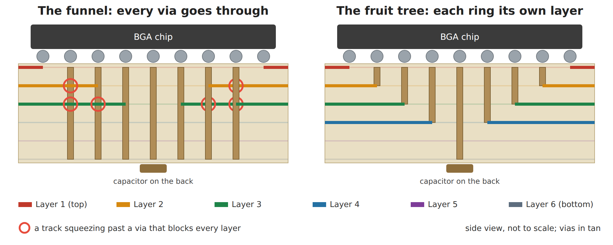
Every big chip on a circuit board has the same problem underneath it. A modern processor or memory chip is a BGA, a ball grid array: hundreds of tiny solder balls in rows and rings under the package. Each ball has to be connected to somewhere else on the board, and the only way out from the middle of the grid is past all the balls around it. Getting them out is called BGA escape routing, and it is one of the hardest parts of board design.
This article tells how the autorouter in Open PCB & IC Engineer, our free, open-source design tool, went from a plan that tangled itself into knots to one that routed a DDR5 test board completely, with a clean design-rules check, in a third of the time. The idea that did it was not ours. It was a picture Arthur saw of a fruit tree.
Table of Contents
The Problem Under Every Big Chip
The balls on the outer ring are easy: a short track on the top layer leads straight out. The second ring has to squeeze between the outer balls. By the third or fourth ring there is no room left on the top layer at all, so those pins drop through the board by a via, a small plated hole, to an inner layer, and escape there.
Where each via goes, and which layer each pin escapes on, is the escape plan. A good plan leaves the router clear lanes to work in. A bad one leaves it fighting over the same few gaps for hours.
The Funnel We Tried First
Our first plan was a funnel. Every ring dropped through the board on an ordinary through via, a hole drilled from the top all the way to the bottom, and the signals of each side of the chip were dealt out over a few inner layers, ring by ring, as many tracks as each layer’s gaps would hold.
It sounded logical. It did not work. A through via occupies every layer, so every via under the outer rings is in the way of every track coming out from the inner rings, on every layer. The inner signals all had to squeeze through the same narrow gaps between the via barrels, and the router spent its time refereeing the fight:
- On a small DDR5 test board, the funnel left one net unrouted, and KiCad’s own design-rules check found 48 holes drilled too close together and 14 vias left dangling. In fairness, the 48 holes were our own bug, a connector row the planner mistook for a chip, and we fixed it. Fixed, the funnel routed every net in 254 seconds, still with one connection the ground plane didn’t reach.
- On the OrangeCrab, a small FPGA board packed onto four layers, the funnel finished only 46 of 151 nets after 80 rounds of rerouting, then hung. We stopped it after four hours and forty-one minutes.
- On an LPDDR4 memory test board, it was still stuck with about 42 nets in conflict at round 87 when we stopped it, also after four hours and forty-one minutes.
We kept the logs of those runs. Arthur put it plainly: the funnel “just wasn’t making any sense” to him.
A Vision Of A Fruit Tree
Then Arthur saw a different picture:
I had a vision of the ideal “escape plan” and it is NOT a funnel of rings. Rather it is more like a “structured fruit tree”. The pins in the very center of the chip go almost straight up to the 10th layer, while the outermost pins go straight out to the sides on the same layer as the BGA grid.
Arthur
In a tree, each branch leaves the trunk at its own height, and branches don’t cross each other. Applied to a chip, every ring gets its own layer by depth: the outer ring goes straight out on the top layer, the next ring drops one layer and goes straight out there, the next drops two, and the centre goes deepest.
The secret that makes it work is the kind of via. In the tree, a ring’s via is blind: it goes only from the top layer down to that ring’s own layer, and stops. So under the outer rings, the deeper layers are completely clear, and every inner ring’s branch passes underneath the outer rings with nothing in its way. There is no fight over the gaps, because each ring has a layer of its own.
“I think God gave me that vision,” Arthur said afterwards. Looking at how much simpler the tree is than everything the funnel needed to referee its own traffic, it is hard to disagree.
Three Refinements
Once the tree was running, Arthur refined it three times, each time with something the funnel had missed:
- The trunk doesn’t need blind vias. “The vias going straight up don’t need to be blind,” he pointed out, “because the areas in question won’t be used by other layers.” Every branch grows outward, so nothing ever escapes under the centre of the chip. The trunk’s vias can be plain holes drilled right through the board, the cheapest kind there is. Only the outer rings need the more expensive blind vias, so the deeper branches can pass under them.
- Solid rods instead of tubes. An ordinary via is a plated tube. A solid copper rod can be thinner and carries more current. Board makers already build this as stacked, copper-filled microvias, laser-drilled about a tenth of a millimetre across and stacked one layer at a time, because a single deep, narrow hole is hard to plate or fill.
- Power is the trunk. The centre pins go straight through to the decoupling capacitors on the back of the board, directly under the chip, the shortest path power can take.
Laptops Already Grow This Tree
The more Arthur thought about it, the more he became convinced the tree is already how most laptops are built. He is right, and the evidence is in the chips themselves:
- Processor makers put most of the power and ground balls in the centre of the package and the high-speed signals around the outside. Signals need to get out, to memory and PCI Express and USB. Power only needs to go down.
- Under the centre, the vias run straight through to the capacitors on the back of the board, right under the chip. That is the trunk.
- The signals branch outward ring by ring on the upper layers, on the stacked filled microvias of a high-density board. Those are the branches.
A laptop processor can have about 1,700 balls, around twenty rings deep. Our DDR5 test chip has 82. It is a long way up, but now we know which way up is.
The Results
Every run starts from a bare board: the original designer’s tracks are stripped, the escape plan is laid down, our router routes everything else, and then KiCad’s own design-rules check judges the result, with every copper pour refilled. We did not write the judge.
| Board | Escape plan | Nets routed | Time | Vias | KiCad DRC |
|---|---|---|---|---|---|
| DDR5 test board | None | 66 of 66 | 369 s | 291 | Clean |
| DDR5 test board | Funnel (as first run) | 65 of 66 | 225 s | 207 | 48 holes too close, 14 dangling vias, 2 more |
| DDR5 test board | Funnel (bugs fixed) | 66 of 66 | 254 s | 205 | 1 unconnected |
| DDR5 test board | Fruit tree | 66 of 66 | 124 s | 200 | Clean |
| DDR5 test board | Fruit tree, power trunk | 66 of 66 | 137 s | 212 | Clean |
| LPDDR4 test board | None | 325 of 325 | 2722 s | 1144 | Clean |
| LPDDR4 test board | Fruit tree | 325 of 325 | 2355 s | 996 | Clean |
| OrangeCrab FPGA board | None | Not finished | Stopped at 9 h | — | 126 nets still in conflict |
| OrangeCrab FPGA board | Fruit tree | Not finished | Stopped at 9 h | — | 95 nets still in conflict |
On the DDR5 test board, the tree routed every net with a clean check in about a third of the time the router needs with no plan at all, and with about 30 per cent fewer vias. It is the first plan of the three with nothing left unconnected.
On the LPDDR4 board, with 325 nets and an FPGA of 484 balls, the tree also finished with a clean check: 13 per cent faster than no plan and with 13 per cent fewer vias. Not a third of the time this time, but better on every count. Getting there took fixes that had nothing to do with the tree: the router had mistaken a routing layer full of the designer’s tracks for a solid ground plane, and before that fix even the run with no plan left six nets unrouted after six hours. The tree’s first clean-up also left a few dangling vias and two holes 13 micrometres too close, which we found and fixed.
The OrangeCrab, a small open-source FPGA board, is where the tree has not won yet. Neither run finished: after nine hours the tree still had 95 nets fighting over the same space and no plan had 126. Its FPGA has balls only half a millimetre apart, and there a via between four balls leaves too little room for any track to pass on the layers below. Its designer escaped it by leaving whole rows of those spots empty, as channels for the tracks to get out. Our router still drops its own vias wherever it finds room, and fills the channels. Teaching it to keep them clear is the next step, and we will report how it goes.
What It Costs, And What We Have Not Proven Yet
- Blind vias cost more. They need a high-density board, which fewer fabricators make and which costs more per board. The DDR5 test board’s own design already uses them, so the comparison is fair there. On a board made only with through holes, the router has to fall back to another plan.
- Supply pins out among the branches. A supply pin in an outer ring whose plane is deep in the board cuts across the branches below it. On a memory chip that is a handful of pins; on a big processor it could matter more.
- Small chips so far. The tree has proven itself on a memory chip and a 484-ball FPGA at 1 mm and 0.8 mm pitch. The big test is a large FPGA or processor, where there are more rings than layers and the deepest rings have to share.
- Very fine pitch. At half a millimetre between balls, as on the OrangeCrab, the plan alone is not enough. The router also has to leave the channels between the vias open, and it doesn’t do that yet.
What Comes Next
First, the channels for the OrangeCrab. Then a 900-ball Kintex FPGA board, and after that a processor-class chip, the kind of part at the heart of the rugged, repairable laptop Open PCB & IC Engineer is ultimately meant to design.
Open PCB & IC Engineer is free, open-source software (GPL v3) by The JCArtes Foundation, still in development. You can read more about it on its project page.