Today we are opening the doors to the Open PCB & IC Engineer beta. Open PCB & IC Engineer, our free, open-source design tool, is ready for its first beta testers. Version 0.2 is the first build we are putting in other people’s hands, and the main reason is its autorouter, the part of the program that lays copper tracks between the parts of a circuit board on its own. We have spent the past weeks teaching it to route boards the way a careful designer would, judged by noise, timing and return paths as well as by whether every connection was made. Now we need people who design real boards to try it on theirs.
This article is two things at once. It announces the beta and tells you how to join it. It is also a step-by-step training guide for first-time users: how to install the program, how to find your way around its windows, how to route your first board, how to check and fix the result by hand, and how to tell us what went well and what did not. If you have used KiCad before, you have everything you need to follow along. If you have not, you can still follow the tour and the first routing exercise, using a demonstration board that comes free with KiCad.
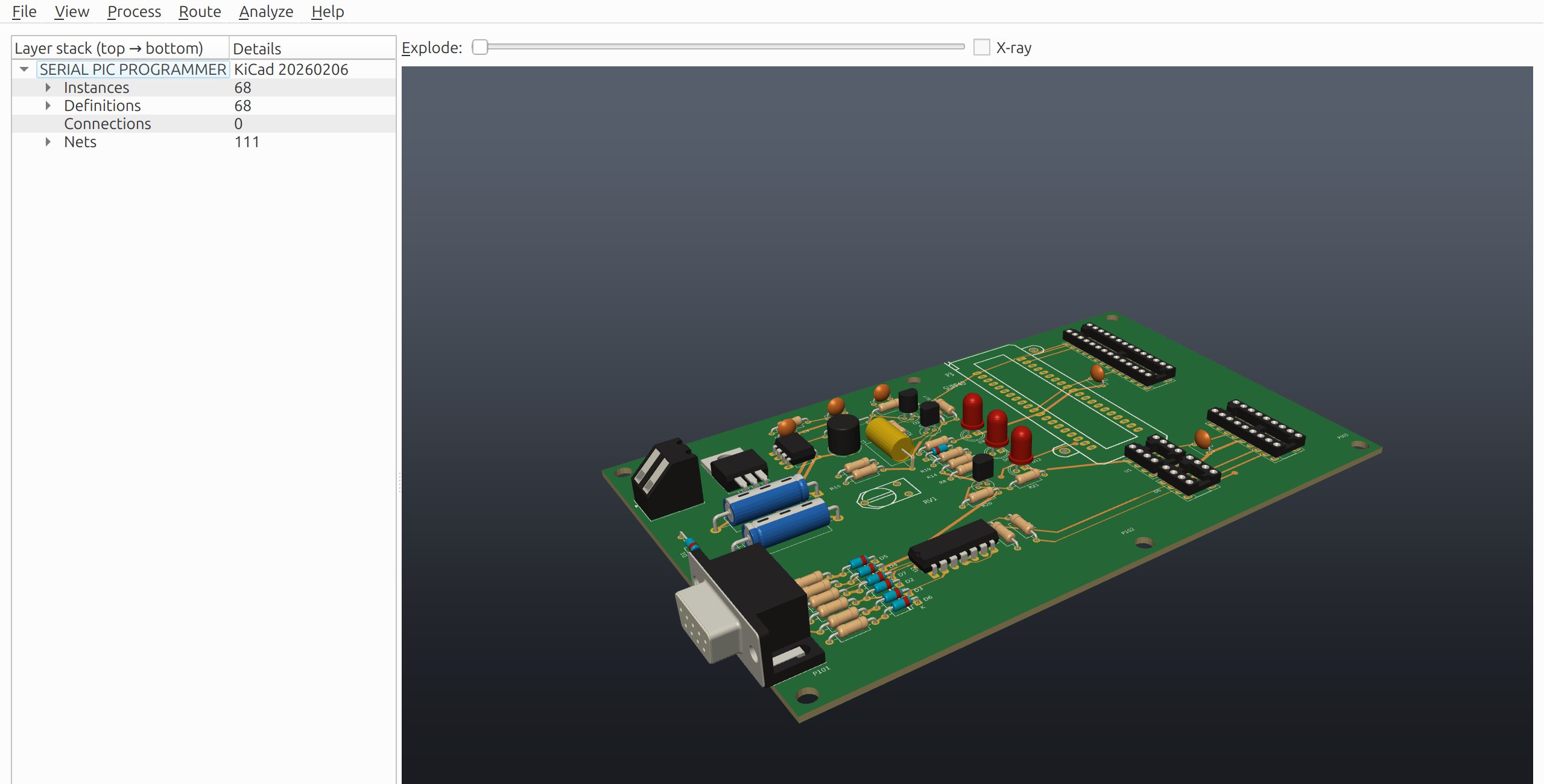
Table of Contents
What Open PCB & IC Engineer Is
Open PCB & IC Engineer, PCBICEng for short, is design software that treats printed circuit boards and integrated circuits as one 3D stack. A modern product is not just a board. It is chips on interposers inside packages on a board, and problems cross those boundaries all the time. PCBICEng reads KiCad boards, chip assemblies in the 3Dblox format and chip layouts in GDSII, and shows them together in one 3D view.
It is not a replacement for KiCad. You still draw your schematic and place your parts in KiCad. PCBICEng reads the board KiCad saves, and it gives you three things KiCad does not:
- An autorouter that judges quality, not just completion. It routes the board, then checks crosstalk between neighbouring tracks, return paths through the planes, and the timing of pairs and buses, and it reroutes the nets that fail. It matches the lengths of differential pairs and bus lines, straightens wavy tracks, and fills the copper pours.
- The Virtual Taping Desk, a place to look at a routed board layer by layer, find its problems and fix them by hand, the way boards were once taped up on light tables.
- A 3D view of the whole stack, from the board down into the layers of a chip, with tools to analyse a chip’s power grid and the path power takes from a regulator to a chip.
A note on the IC side. The chip-design part of PCBICEng, everything to do with integrated circuits, packages and the stack inside them, is just beginning. You can open chip assemblies and layouts and look around them, but that work is not ready for testing yet, and this beta does not ask you to test it. The beta is about the board side: the autorouter and the Taping Desk. We will open the IC side to testers when it is ready, and we will say so.
PCBICEng is free software under the GNU General Public License, version 3. Everything you receive in the beta, you receive under that licence.
Why A Beta, And Why Now
We have tested the router on 23 boards designed by professionals, from small KiCad demonstrations to a 902-net FPGA board, and every result was judged by KiCad’s own design-rules check (DRC), not by a checker we wrote ourselves. We wrote about what that taught us, mistakes included, in 30 Honest Lessons From Building an Open Source PCB AutoRouter.
But 23 boards are 23 boards. Every new board we tried taught the router something, and the boards that will teach it most are the ones we have never seen: yours. A beta is how we find out where it falls short on real work, while the people trying it know it is still being built.
So please treat version 0.2 as what it is. It is for testing, not for production. Never send a board to a factory without opening it in KiCad and running KiCad’s own DRC first, with the pours refilled. The router tells you honestly what it could not finish, and the Taping Desk shows you its problems, but the last word belongs to KiCad and to you.
How To Join The Open PCB & IC Engineer Beta
Joining takes about a minute, right here on this page.
- Fill in the form below with a username and your email address. If you like, add a line about what kind of boards you design. That helps us know which parts of the router you will exercise.
- Check your email. The website sends you a link to set your password. Set it, and you are a beta tester.
- Sign in at JCArtes.Org with that account. Signed in, the download links in this article work for you.
Already have a JCArtes.Org account? Sign in first, and the form becomes a single Join The Beta button.
Why an account instead of a public download? Because we want to hear from you. A beta that thousands download and nobody reports on teaches us nothing. With an account, we know who is testing, we can tell you when a new version is out, and you have a direct line to us when something goes wrong.
An Application Password For Git
If you plan to get the source code with git, make an application password as well. It is a separate password just for git, which you can revoke at any time without changing your main password.
- Sign in at JCArtes.Org and open your Profile page.
- Scroll down to Application Passwords.
- Type a name for it, such as “git”, and click Add New Application Password.
- Copy the password it shows you. It is shown only once.
When git asks for a username and password, give your JCArtes.Org username and this application password. Your normal account password works too, but the application password is safer, because you can throw it away on its own.
Getting The Software
There are two ways to get version 0.2: a ready-to-run program for Linux, or the source code to build yourself.
The Ready-To-Run Linux Program
The Linux program is a single download that carries everything it needs inside it, including Qt and OpenCASCADE, so you do not have to install anything else.
- What you need: a 64-bit Intel or AMD computer running Linux, new enough to have glibc 2.38 or later. That means Ubuntu 24.04 or newer, Linux Mint 22 or newer, Debian 13, Fedora 39 or newer, or anything of the same age. You need working OpenGL graphics for the 3D view, which any desktop with ordinary graphics drivers has.
- The download: pcbiceng-0.2-linux-x86_64.tar.gz, about 49 MB, for signed-in beta testers.
- Its checksum: SHA256SUMS.
Once it has downloaded, open a terminal in your Downloads folder and check that the file arrived whole:
sha256sum -c SHA256SUMSIt should say “pcbiceng-0.2-linux-x86_64.tar.gz: OK”. Then unpack it and start it:
tar -xzf pcbiceng-0.2-linux-x86_64.tar.gz
cd pcbiceng-0.2-linux-x86_64
./bin/pcbiceng
That is all it takes to run it. If you want it in your applications menu, run ./install.sh from the same folder. It installs for your account only and does not need sudo. To install it for everyone on the computer, run sudo ./install.sh –system, which puts it in /opt. To take it out again, run the same command with –uninstall added.
A Windows version exists in our build scripts, but it is not part of this first beta. We will add it once the Linux beta has settled.
The Source Code
The source lives in a git repository on JCArtes.Org, open to beta testers:
git clone https://jcartes.org/git/pcbiceng.gitGit asks for your username and password: give your JCArtes.Org username and the application password you made. If you would rather not type it every time, tell git to remember it for an hour:
git config --global credential.helper "cache --timeout=3600"To build it, you need a C++20 compiler (GCC 13 or newer works), CMake 3.24 or newer, and Qt 6 with its Widgets and OpenGL modules. We build with Qt 6.11. OpenCASCADE is optional: with it, parts are drawn from their real 3D models, and without it, they are drawn as simple shapes. From the folder you cloned:
cmake -S . -B build -DCMAKE_BUILD_TYPE=Release -DCMAKE_PREFIX_PATH=/path/to/Qt/6.11.2/gcc_64 -DPCBICENG_WITH_OCCT=OFF
cmake --build build -j
The program is then build/pcbiceng. If you have OpenCASCADE installed, leave out the last option and point -DOCCT_ROOT at its install folder instead. The repository holds everything else too: the full plan in PLAN.md, and the complete record of the router’s development, mistakes included, in docs/autorouting-notes.md.
When we publish a new version, git pull brings your copy up to date.
A Tour Of The Main Window
Start the program and open a board with File > Open (Ctrl+O). It reads KiCad boards (.kicad_pcb), 3Dblox chip assemblies (.3dbx) and GDSII chip layouts. For this tour, any KiCad board will do. If you have KiCad installed, its demonstration boards are a good start; we will use one in the next section.
The main window has four parts.
- The layer stack on the left lists what you opened: the board, its parts (instances), their definitions, the connections between them and the nets. Click the small arrows to look inside.
- The 3D view in the middle shows the whole design.
- The message panel under the view reports what the program read and anything it could not. A part whose 3D model is missing is drawn by its pads and silkscreen, and the panel tells you which ones.
- The Explode slider and the X-ray box above the view. Explode pulls the levels of the stack apart, so you can see between the board, a package and the chip inside it. X-ray (Ctrl+T) makes parts see-through.
Moving Around In 3D
You can move around entirely with the mouse:
- Left drag orbits around the point you pressed on.
- Right drag pans: the spot you grabbed stays under the cursor.
- The wheel zooms toward whatever is under the cursor.
- Double-click glides in to the spot you clicked. Double-click empty space to go back to the start.
- Left click selects a part, or lights up a net when you click on copper.
The keys help too, once you have clicked in the view. 1 to 5 switch to the top, bottom, front, side and 3D views. F frames the selected part. Home or Ctrl+0 glides back to where you started. The arrow keys orbit, and Shift with the arrows pans.
You never need to memorise any of this. Help > Controls (F1) opens a page with every mouse and key control, and you can leave it open beside the window while you try them.
The Menus
- File opens and saves designs, places a 3Dblox chip assembly into a board part, and loads a chip layout into a die.
- View has the camera views, X-ray, framing, walk mode, named areas, and Export Shareable Model, which makes a copy of a design you can give to customers with the chip layouts replaced by density maps.
- Process describes how parts are made and mounted (their materials, bonding and underfill) in the terms of the JEP30 standard.
- Route holds the two tools most of this guide is about: Autoroute Board (Ctrl+R) and the Virtual Taping Desk (Ctrl+Shift+T).
- Analyze holds the power and signal analyses, which we come back to near the end.
Your First Autoroute, Step By Step
The best way to learn the router is to watch it route a board you can check. We will use the PIC programmer, one of the demonstration boards that come with KiCad. It is a real two-layer board with 34 nets to route, and because it is KiCad’s own, everyone has it and everyone can compare.
Step 1: Copy The Demonstration Board
KiCad installs its demonstration projects alongside the program. On most Linux systems they are in /usr/share/kicad/demos, and the board we want is in the pic_programmer folder. In KiCad’s project window, File > Open Demo Project takes you there too.
Copy the whole pic_programmer folder somewhere of your own, such as your home folder. Work on the copy, never on KiCad’s originals. The folder holds the board (pic_programmer.kicad_pcb), the project file (pic_programmer.kicad_pro), and the schematic.
The project file matters more than it looks. It holds the board’s net classes and design rules: track widths, clearances and via sizes. PCBICEng reads them from there. A board opened without its project file is judged against KiCad’s default rules instead, and the results will look wrong. Whenever you copy a board, copy its .kicad_pro with it.
Step 2: Take The Tracks Off
The demonstration board is already routed by hand. To give the router something to do, open the copy in KiCad’s PCB editor and remove its tracks and vias:
- Choose Edit > Global Deletions.
- Tick Tracks and Vias, and nothing else. Leave the zones, footprints and drawings alone.
- Click OK, then save the board with File > Save.
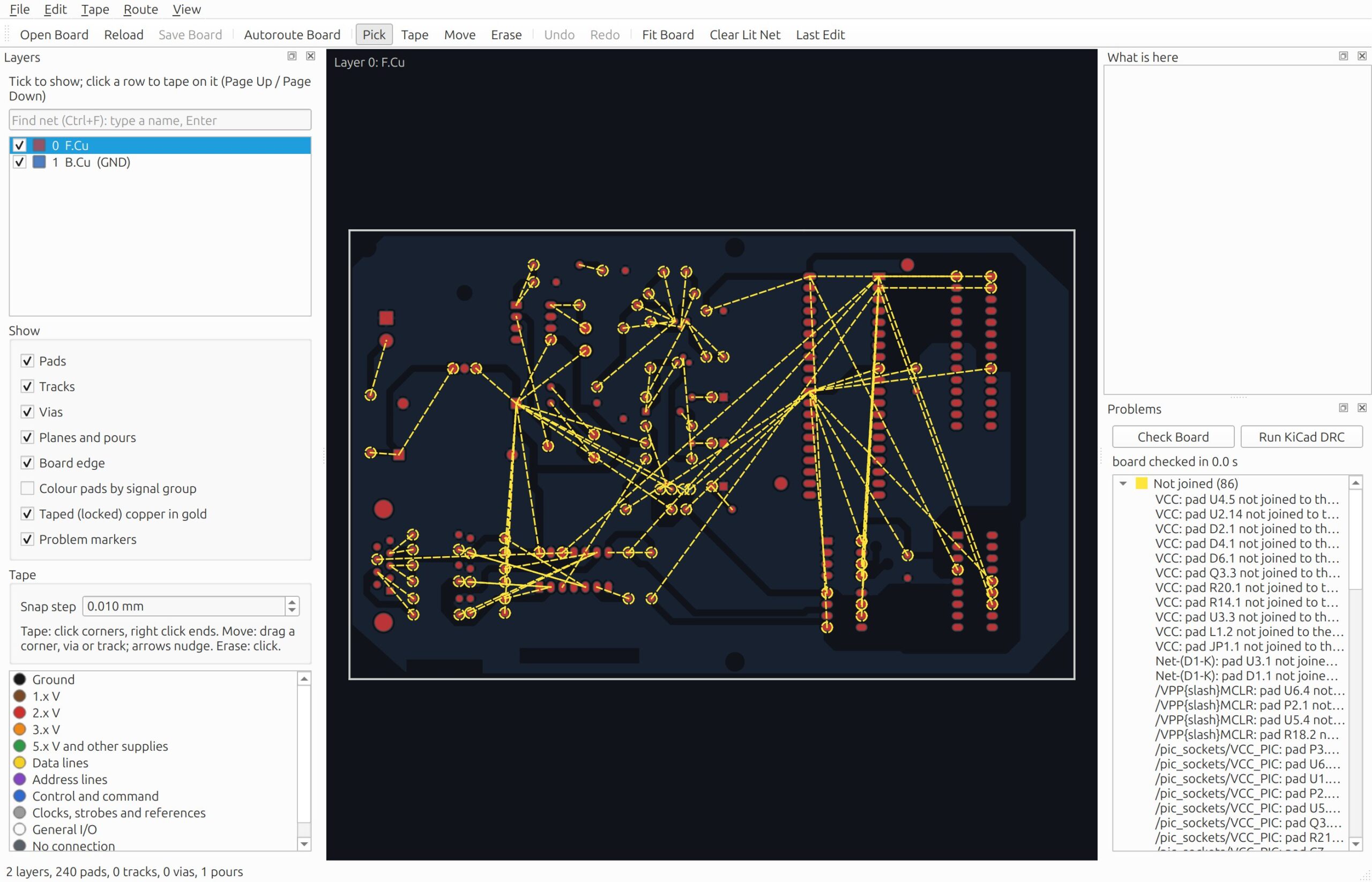
The board now has its parts in place and nothing joining them, except the ground pour on the bottom layer. You can see the result on the Taping Desk below: pads, the board’s edge and the pour, and thin lines showing which pads must be joined.
Step 3: Start The Autorouter
In PCBICEng, choose Route > Autoroute Board (Ctrl+R). It opens the Virtual Taping Desk and asks for a board, if one is not open already. Choose your copy of pic_programmer.kicad_pcb.
The router then asks where to save the routed board. It suggests the same name with -routed added, pic_programmer-routed.kicad_pcb, beside the original. Accept it. The router never writes over the board you gave it. It always routes into a new copy, and it copies the board’s project file, and any budget or custom rules file, beside the copy, so the copy keeps its rules.
A progress window appears with a bar and a line of plain words saying what the router is doing: building its grid, negotiating between nets, checking noise, length matching, and so on. On the PIC programmer, the whole thing takes a few seconds. A big board can take hours. The Stop button stops the router wherever it is, and in that case nothing is written.
Step 4: Read The Result
When the router finishes, it tells you what it did in one line. On the PIC programmer:
Routed into pic_programmer-routed.kicad_pcb: 34 of 34 nets, 125 of 125 connections, 1816 mm of track, 6 vias, 0.1 minEvery net routed, every connection made. If some nets could not be finished, the same window lists them by name, with the reason the router gave up, so you know exactly where to look. Click Show Details to see the router’s full notes: how many rounds it took, which nets it rerouted for noise, how much it straightened, and how the pours were filled. Those notes are the most useful thing you can send us when something goes wrong.
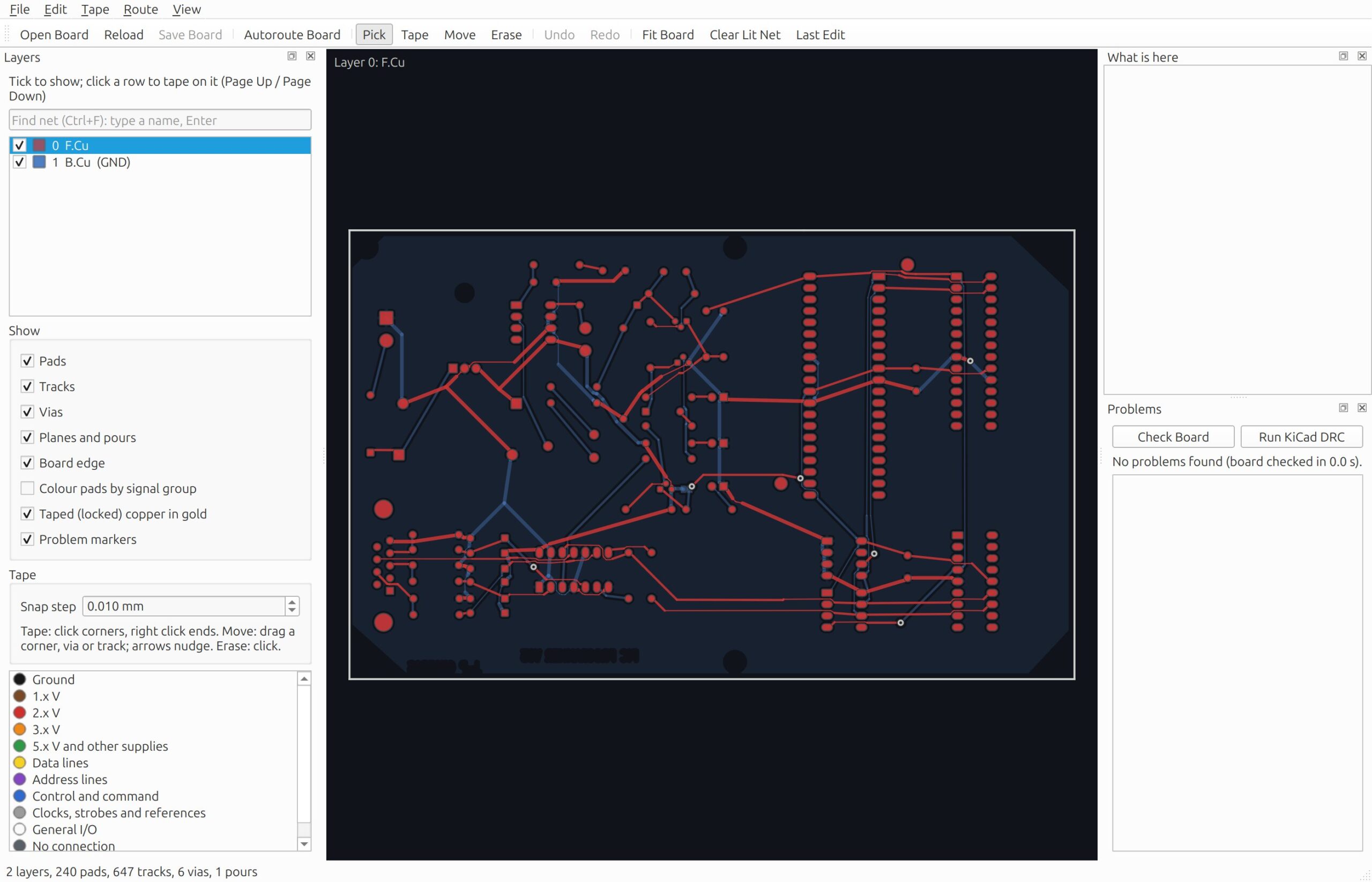
Then the routed copy opens on the Taping Desk.
Step 5: Check It Yourself
The Taping Desk checks the board as soon as it opens it. The Problems panel on the right says “No problems found” on our run of the PIC programmer. That check covers clearances, pads that are not joined to their net, and tracks cutting through a plane, and it takes a second or so.
Then check it with KiCad, which is the final judge. On the Taping Desk, Run KiCad DRC runs KiCad’s own check, with the pours refilled, and lists its findings in the same panel. It needs KiCad’s command-line tool, kicad-cli, which comes with KiCad, including the Flathub version. On a big board it takes minutes. Or open the routed copy in KiCad itself, choose Inspect > Design Rules Checker, make sure Refill all zones before performing DRC is ticked, and run it.
That is your first autoroute. The rest of this guide shows you how to steer the router, and how to fix by hand what it could not do.
Reading The Router’s Notes
Every routing leaves notes behind: in the Show Details part of the result window, on the terminal with pcbiceng –autoroute, and in the .route.txt file beside the routed copy. They look technical at first, but they tell a story you can learn to read in a few minutes. Here are the notes from the PIC programmer, in order, with what each one means.
Grid on the board's lattice: 0.127 mm (89 % of its points), not 0.125The router lays a grid of cells over the board and searches for paths from cell to cell. It noticed that this board was drawn in inches, with 89 % of its pads and corners on a 0.127 mm (5 mil) lattice, so it put its grid on that lattice instead of a round metric one. Paths then line up with the way the designer drew the board.
138 tight pads: tracks neck down within 4 mm of them, where they mustSome pads are too close together for a track of the full class width to pass between them. Within 4 mm of such a pad, a track may become narrower, but only where it has to.
Round 1: 15 nets in conflict ... Round 5: 0 nets in conflictThis is the heart of the router. In the first round, every net takes the path it likes best, even if it has to share cells with another net, and 15 nets ended up sharing. Each round, the shared cells become more expensive, so nets move to make room for each other, until no two nets share a cell. On a small board this takes a handful of rounds. On a big one it can take a hundred or more. If the count stops falling for a long time, the router says so in a note that starts with “Self-watch”, naming the layers, parts and nets where it is stuck.
Exact spacing: 132 pairs too close after the grid, 0 after moving 218 corners and vias off itA grid can only place copper in whole cells, so some tracks end up a few micrometres too close. The exact pass moves corners and vias off the grid until every clearance is met. “0 after” is what you want to see. If a number is left, the router routes those nets again, and anything it cannot fix ends up among the nets it names as not finished.
Noise: as routed, 0 of 28 nets over budgetAfter routing, the router checks every signal against its budget for crosstalk and return paths (explained in the next section). Nets over budget are routed again with their noisy neighbours made more expensive, and the result is kept only if it is better.
Meanders: 0 pairs and groups, 0 nets lengthenedThe length matching. This board has no differential pairs and no budget file, so there was nothing to match. On a board with pairs or bus groups, this line says how many nets were lengthened and by how much.
Straightened: 9 segments fewer, 1.45 mm shorterThe final clean-up: runs of short, slightly wavy pieces are pulled into straight lines wherever a straight line keeps its clearances.
Pours filled: 2 pieces, 117 islands removedThe copper pours, such as the ground pour on this board’s bottom layer, are filled around the new tracks, the way KiCad’s refill does it. An island is a piece of pour that no copper of its own net reaches. KiCad removes those, and so does the router.
routed: 34 of 34 nets, 125 of 125 connections, 1816 mm of track, 6 vias, 0.1 minThe summary. If it is less than everything, look for the lines that start with “not done” below it. Each names a net and says why it was left: “no way through to a pad” (the pad is boxed in, often a placement problem), “too close to another net’s copper” (a near-miss the exact pass could not mend), or “still in conflict” (the negotiation ran out of rounds).
What The Router Checks, In Plain Words
A board can be completely routed and still not work. Tracks that run side by side can disturb each other, a signal can lose its return path, and two lines that should arrive together can arrive apart. Most autorouters do not look at any of this. Ours does, and it helps to know what it is looking at.
Crosstalk
Two tracks running side by side for a long way act like a weak transformer. When one switches, a little of its voltage appears on the other. That is crosstalk, and the router measures it on every pair of neighbouring tracks, from the board’s real layer stack: the thickness of each layer, the dielectric between them, and where the planes are. It reports the noise on each net as a share of the voltage that switched next to it. By default, more than 5 % counts as over budget, and the router moves the net.
Crosstalk is strongest on a layer with no plane next to it, and weakest on a layer sandwiched between two planes. That is one reason the layer stack matters so much.
Return Paths
A signal’s current does not just flow out along its track. It flows back too, through the plane right under the track, following it closely. If the plane has a gap under the track, a split between two supplies or a row of holes, the returning current has to find its way around. That makes a loop, and loops radiate noise and pick it up.
The router checks every signal track against the planes beside it and measures how much of it runs over a gap. By default, more than 1 mm over a gap counts as over budget. It also checks every via that moves a signal from one plane’s side to another’s, to see whether the return current has a way to follow: a ground via nearby, or a capacitor between the two planes.
On a two-layer board like the PIC programmer, half the tracks sit on the ground pour itself, with no plane beyond them, so the router checks gaps there only if a budget file asks it to.
Timing And Length Matching
A signal takes time to travel along a track: roughly 6 to 7 picoseconds per millimetre inside a typical board. For most signals that does not matter. For a differential pair it matters a great deal, because the two halves must arrive together. It matters for a memory bus too, because its data lines are read at the same instant.
The router times each net along its real path, from pad to pad, through every via, and adds meanders to the faster lines until they arrive within their match. A pair is matched to within 5 picoseconds by default. A bus group is matched to its budget file’s match_ps.
Budgets Tie It Together
All three checks become a pass or a fail through the budgets described above. With no budget file, every net is judged against the safe worst case. With one, you tell the router which nets switch together, which never switch, and how much each can stand, and its judgement becomes yours.
Steering The Router
The router has sensible defaults, so on most boards you can just press Ctrl+R. But you can guide it in two ways, both done in files you already understand.
Lock What You Want To Keep
The router keeps every track and via that is locked in KiCad, and routes everything else. Anything unlocked is treated as a suggestion it may throw away, so autorouting a board that is already routed routes all its unlocked nets again.
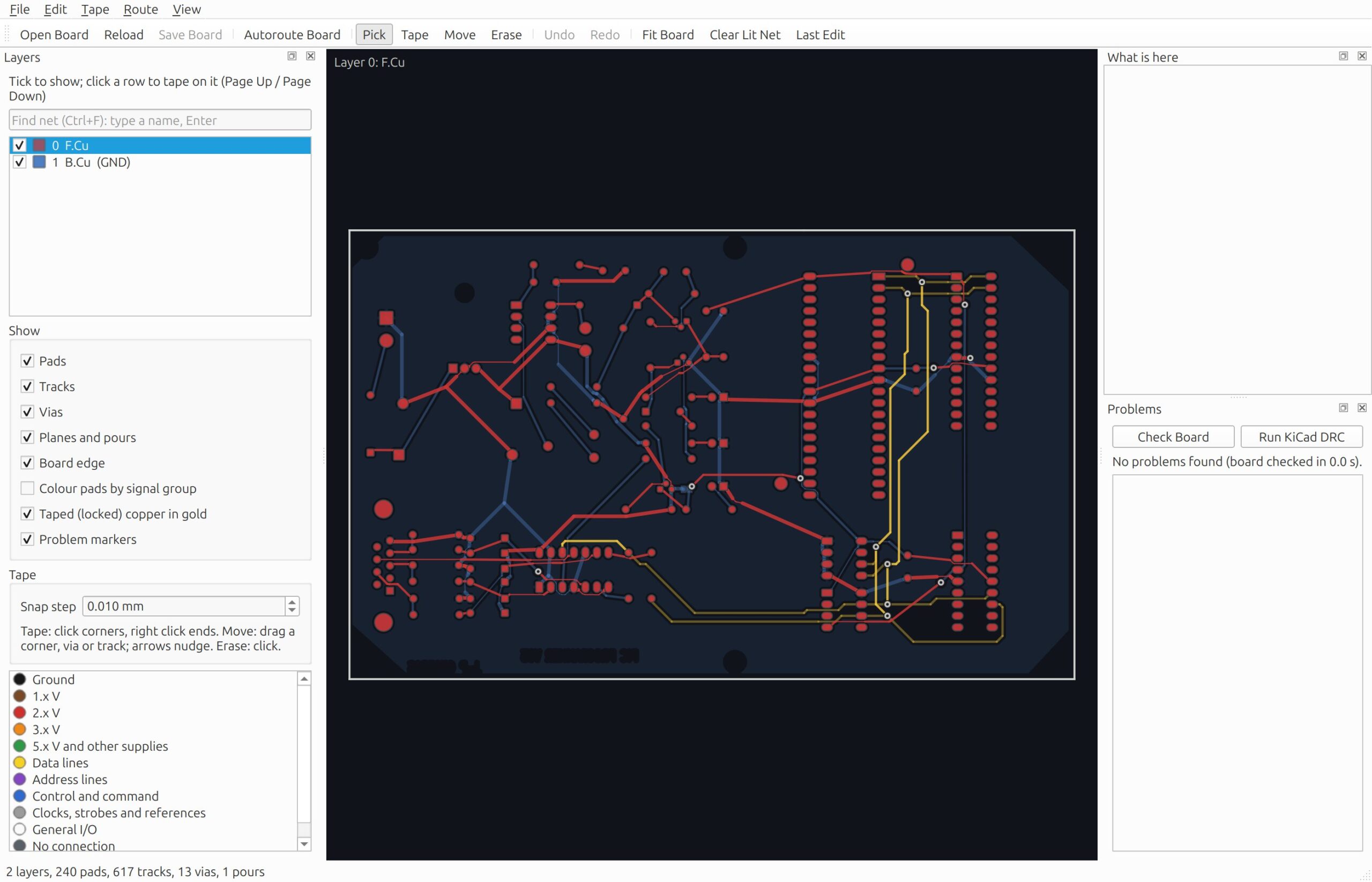
That gives you a simple way to work. Route the critical parts by hand in KiCad first: a clock, a differential pair, the escape from under a big chip. Lock them (in KiCad, select them, then right-click and choose Locking > Lock), save, and let the router do the rest around them. The tracks you locked come through untouched, and the Taping Desk shows them in gold, so you can see at a glance what was yours.
Exercise: Route Two Nets Yourself, Let The Router Do The Rest
Try it on the PIC programmer. Its two programming lines, /CLOCK-RB6 and /DATA-RB7, carry the clock and the data from the PC’s port to the chip being programmed. They are just the kind of lines a designer routes by hand first. This time, instead of deleting every track, keep those two:
- Open a fresh copy of the demonstration board in KiCad’s PCB editor.
- Select all the copper of /CLOCK-RB6 and /DATA-RB7. In KiCad, click a track and press U, which grows the selection along the connected copper; press it again if part of the net is left out, and hold Shift to add the second net.
- Right-click and choose Locking > Lock.
- Choose Edit > Global Deletions, tick Tracks and Vias, and leave any option that includes locked items unticked, so your two nets stay. Click OK and save.
- In PCBICEng, Route > Autoroute Board as before.
On our run, the router finished the other 32 nets around the two you kept: 32 of 32 nets, 114 of 114 connections, 13 vias, and no problems found. Your two nets come through exactly as you left them, in gold on the Taping Desk.
The same method scales to any board. The more of the critical work you do yourself and lock, the less the router has to guess.
Tell It What Your Nets Can Stand
By default, every net is judged against the same worst-case budget: an edge of 1 nanosecond, at most 5 % of noise from its neighbours, at most 100 picoseconds of timing skew, and at most 1 mm of its length over a gap in its reference plane. That is a safe default, but it does not know that your SPI bus is slow, or that your DDR3 byte lanes must arrive within 20 picoseconds of each other.
A budget file tells it. It is a small text file beside the board, named after it: pic_programmer.budget.json for pic_programmer.kicad_pcb. Here is one for a board with a DDR3 memory:
{ "defaults": { "rise_ns": 1, "noise_pct": 5, "skew_ps": 100, "gap_mm": 1 },
"nets": [ { "match": "^RAM_(D[0-7]|LDM|LDQS[+-])$", "group": "lane0", "match_ps": 20, "ends": ["U3", "U4"] },
{ "match": "^/CFG_", "quiet": true } ] }
Each rule picks nets by a pattern on their names (or by net class), and sets what applies to them:
- group names nets that switch together, like the lines of a bus. Crosstalk between members of one group counts as timing skew, not noise, because nobody is listening to the line while it switches.
- match_ps is how far apart in time the group’s members may arrive. The router lengthens the faster ones with meanders until they arrive together.
- ends names the parts the timing runs between, so a stub to a test point does not count.
- quiet marks a net that never switches, such as a configuration strap.
- rise_ns, noise_pct, skew_ps and gap_mm set the net’s own edge and limits.
Differential pairs need no rule at all. The router recognises them by KiCad’s naming (a name ending in P and N, or + and −), routes the two halves side by side at the pair’s gap from its net class, and matches their lengths to within 5 picoseconds.
The Virtual Taping Desk
Before computers, a board was laid out by hand with black tape on clear film over a light table. The Virtual Taping Desk brings back that directness: the board one layer at a time, with tools to look, find, check and fix. Open it with Route > Virtual Taping Desk (Ctrl+Shift+T), then File > Open Board (Ctrl+O). It reopens the last board you used.
Reading The Board
The window has three panels around the board.
- Layers, on the left, lists the copper layers from top to bottom, with the nets poured on each in brackets. Tick a layer to show it, untick it to hide it. Click a row to make it the current layer, the one you tape on; Page Up and Page Down step through them. Below the layers, Show turns pads, tracks, vias, planes and pours, the board edge and problem markers on and off.
- What is here, at the top right, tells you what you clicked: a track, a via, a pad, its net and its layer.
- Problems, at the bottom right, lists everything the checks found.
Move around with the mouse wheel to zoom and a right drag to pan. Fit Board (Home) shows the whole board again.
Two display options make a busy board easier to read. Colour pads by signal group colours each pad by what its net does: ground, each supply voltage, data lines, address lines, control, clocks and strobes, general I/O. The legend at the bottom left uses the resistor colour code. Taped (locked) copper in gold shows everything locked in gold, which separates your work from the router’s.
Finding A Net
Type a net’s name into the Find net box at the top of the Layers panel (Ctrl+F) and press Enter. The desk lights the net, zooms to show all of it, and switches to the layer where most of its track is. It is forgiving about names: “3V3”, “+3.3V” and “3.3 VDC” all find the 3.3 volt supply. Add “near” and a part to see only the part of a net close to it: “GND near U3” shows the ground pads of U3 and the track within 2 mm of them. Clear Lit Net puts it out again.
The Pick tool (P) does the same with a click: click any copper to light its net and see what it is in the What is here panel.
Finding Problems
Check Board runs the desk’s own check: clearances between copper of different nets, pads not joined to their net, and tracks cutting a plane. It takes seconds. Run KiCad DRC runs KiCad’s full check, as described above.
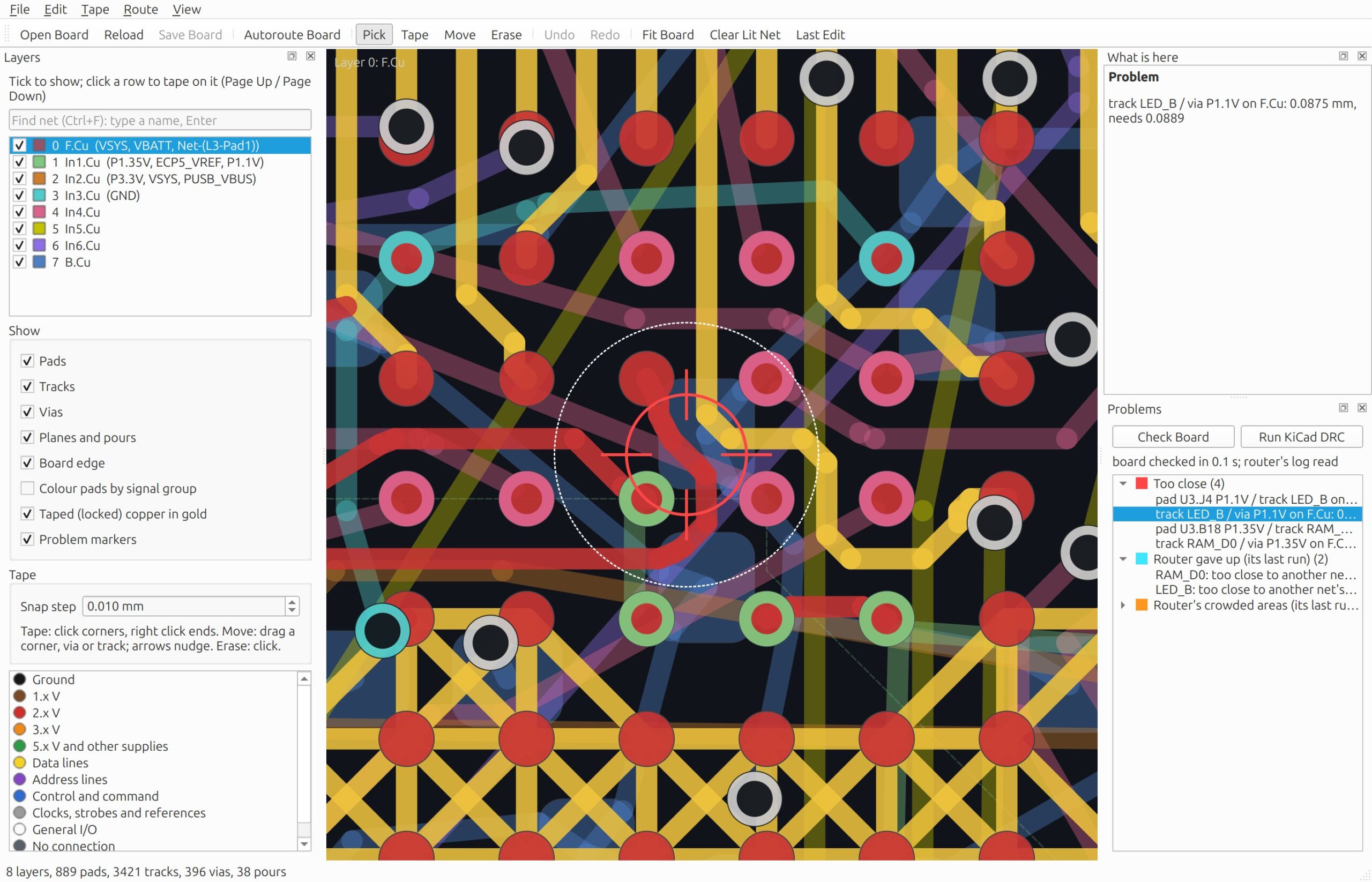
The Problems panel groups what they found. Every routed copy also gets the router’s notes beside it, in a file named after the board with .route.txt on the end. The panel reads them, so it lists the nets the router gave up on, and you can go straight to each one. Click a problem, and the desk takes you there: it switches to the problem’s layer, zooms in, rings the spot and puts a red target on it. The What is here panel then says exactly what is wrong, such as “track LED_B / via P1.1V on F.Cu: 0.0875 mm, needs 0.0889”.
Fixing Things By Hand
The Tape menu has four tools, each with a one-letter key.
- Pick (P) shows what is under the mouse and lights its net.
- Tape (T) lays a new track for the lit net on the current layer. Light the net first with Pick or Find net, choose the layer, then click each corner of the track in turn. A right click, or Escape, ends it.
- Move (M) drags a track’s corner, a via, or a whole track. The arrow keys nudge whatever you picked by one snap step.
- Erase (E) takes out the track or via you click.
The Snap step box sets how far moves and nudges go, and where taped corners land. The default, 0.010 mm, is fine enough for the tightest boards. Set it to 0 to move freely.
While you tape or move, the desk checks your copper as you go. Wherever it comes too close to another net’s track, via or pad, a red target appears with the gap written on it, such as “0.0526 of 0.0889 mm”, and it disappears as soon as there is room. You see the problem while you are making it, not after.
Undo (Ctrl+Z) and Redo (Ctrl+Shift+Z) remember your last 200 steps. Last Edit (L) takes you to your most recent change, on its layer; press it again to go one edit further back.
Everything you tape or move is locked, so the router will keep it if you route the board again.
Saving Your Work
Save Board (Ctrl+S) writes your tracks and vias back into the board file and checks the board again. The first time you save a board, the desk keeps a copy of how it was, beside it, named with .before-taping on the end, so you can always go back. Each save also adds a list of what you changed to a file named after the board with .edits on the end: the time, the layer, the place, and what was done. If you send us a board you fixed by hand, that list tells us what you had to fix, which is exactly what we need to know to improve the router.
If the board changes outside the desk (because you routed it again, or edited it in KiCad), Reload (F5) reads it again.
A Tip From Our Own Testing
When a hand fix keeps failing in one small spot, the net in the error message may not be the one that should move. On one of our test boards, three nets were fighting over a channel 0.8 mm wide, and the fix was to move a different net out of the way. When something will not fit, list every net in that channel and ask which one could go somewhere else.
Going Deeper In 3D
The beta’s purpose is the router and the Taping Desk. The rest of the program is there for you to look at, but remember the note at the start: the IC design side is just beginning and is not ready for testing yet. What follows is a quick look at where it is heading, not a list of things we are asking you to test.
- Explode and X-ray. Drag the Explode slider to pull the stack apart: the board, its packages, and the chips inside them, each at its own height. Tick X-ray to see through parts.
- Walk mode. In a chip’s layout, press W to walk down the “hallways” between the shapes of a chip layer, as if you were standing inside the chip. The wheel walks you forward and back, the arrow keys turn at the next opening, and Page Up and Page Down ride an elevator between the metal layers. Escape, W or Home brings you back.
- Named areas. View > Go to Area (Ctrl+G) takes you to a named part of a layout, such as one block of a chip, or a place you named yourself.
- Placing chips. File > Place 3Dblox Assembly in Selected Part puts a chip assembly into a board part, which becomes its package. Load Chip Layout (GDS) into Selected Die draws a chip’s real layout inside a die, each process layer at its own height.
The Analyses
The Analyze menu has three analyses. They work on designs with chip layouts and power nets, so they will not do much on a plain two-layer board, but they show where the program is heading.
- Power Grid (IR Drop) solves a chip’s power network and shows the voltage drop and the current as a heat map against each layer’s limits. Rest the mouse on the map to read the values.
- Power Path (Regulator to Chip) follows a supply from its regulator through the board, its decoupling capacitors and the package to the chip. You can mark parts as failed and see how the chip’s supply changes.
- Signal Net (Switching) shows a net rising and falling: the current charging its wires and the gates it drives, how far each place lags behind the driver, and the wire’s delay.
The Command Line
Everything the Autoroute menu does is also available from a terminal, which is handy for routing several boards in a row or on a computer with no screen:
pcbiceng --autoroute pic_programmer-routed.kicad_pcb pic_programmer.kicad_pcbThe first file is the new routed copy, and the second is the board to route. It prints its progress, the router’s notes and the same one-line summary as the menu, then lists any nets it could not finish. It does exactly what the menu does, including copying nothing over your original. (It does not copy the project file for you: copy the .kicad_pro beside the routed copy yourself before you check it.)
Another option opens a board straight onto the Taping Desk:
pcbiceng --taping-desk pic_programmer-routed.kicad_pcband pcbiceng –help lists the rest.
Your First Week As A Tester
If you are not sure where to start, here is a plan that takes an hour or two spread over a few days, and gives us the reports that help most.
Day one: the demonstration board. Install the program, then do the two exercises above on the PIC programmer: route it from blank, then route it around two locked nets. Open both results in KiCad and run its checker with the pours refilled. You will learn the whole loop on a board where you know what a good result looks like, and if anything in the installation or the exercises trips you up, that is our first report.
Day two: a board of your own that you know well. Pick a finished board you routed by hand, ideally a small one. Copy it with its project file, take the tracks off, and let the router route it. Then compare: open your original and the routed copy side by side in KiCad. Where did the router go a different way from you? Was its way worse, or just different? Did it finish? Write down what surprised you.
Day three: the Taping Desk. On a routed board, open the Taping Desk and walk through it: find a net or two by name, colour the pads by signal group, check the board. If the router left anything unfinished, try finishing it by hand with Tape and Move, then save. If it finished everything, practise by erasing a track and taping it again. Tell us what was easy and what was awkward.
Day four: something hard. If you have a board with a BGA, DDR memory or differential pairs, try that next, with a budget file if the board needs one. Expect it to take longer, and expect the router to struggle in places. Those struggles are exactly what we want to see.
Any day: write to us. A report does not have to be long. Three sentences about what you did and what happened is enough to start a conversation.
When Something Goes Wrong
Here are the problems you are most likely to meet, and what to do about each.
The message panel says “No project file” and the results look strange. PCBICEng read the board without its .kicad_pro beside it, so it used KiCad’s default rules instead of your board’s. Copy the project file into the same folder as the board, with the same name, and open it again. The router copies it beside every routed copy for you, but a board you copied yourself needs it too.
Some nets are “not done”. Read the reason in the result window or the .route.txt file. “No way through to a pad” usually means the pad is boxed in, by parts placed too close or by your own locked copper: check the spot on the Taping Desk, where the problem list takes you straight there. “Too close to another net’s copper” is a near-miss of a few micrometres, often fixable by hand with Move. “Still in conflict” means the negotiation ran out of rounds, and routing again after locking what came out well often finishes it.
Routing is taking a very long time. Watch the progress line. If the number of nets in conflict is still falling, the router is getting there. If a “Self-watch” note says it has stopped improving, press Stop, look at where it says it is stuck, and help it there: route those nets by hand and lock them, or move a part to make room.
Parts are drawn as flat outlines in 3D. Their 3D models were not found. The message panel lists them. PCBICEng looks for models where KiCad does, through KiCad’s model path settings, and you can point it at your models with the PCBICENG_KICAD_3DMODELS environment variable. A missing model never affects routing.
Run KiCad DRC says kicad-cli was not found. The button uses KiCad’s command-line tool. Install a current KiCad from your distribution or from Flathub (we test with KiCad 10), and the button finds it. Or open the board in KiCad and run its checker there.
The program does not start. Run it from a terminal (./bin/pcbiceng) to see the message. A line about GLIBC means your Linux is older than the program needs; see the requirements above. A line about OpenGL means the graphics driver is missing or the program is running without a desktop; the 3D view needs real graphics.
The checksum does not match. The download was cut short or damaged. Download it again.
Git keeps asking for a password, or says 401. Check the username, and use an application password from your Profile page. A 403 means you are signed in, but the account is not a beta tester yet: sign in on this page and click Join The Beta.
A download link shows “Beta testers only”. Sign in at JCArtes.Org with your tester account first, then open the link again.
A Short Glossary
If some of the words in this guide are new to you, here is what they mean.
- Net: a set of pins that must be joined electrically, such as every pin that connects to ground.
- Track: a strip of copper joining pins on one layer of the board.
- Via: a small plated hole that carries a connection from one layer to another.
- Pour, or zone: an area of copper filled automatically around everything else, usually for ground or a supply.
- Plane: a pour that covers most of a layer, giving the signals beside it a reference and a return path.
- Layer stack: the order of the copper layers and the insulating layers between them.
- Clearance: the smallest gap allowed between copper of two different nets.
- Net class: a group of nets that share a track width, clearance and via size, set in the board’s project file.
- DRC: the design-rules check, which finds every place a board breaks its rules.
- Differential pair: two nets carrying one signal as opposites, such as USB’s D+ and D−, routed side by side.
- BGA: a chip with its connections as a grid of solder balls underneath, the hardest kind of part to route around.
- Crosstalk: the noise one track puts on its neighbour when it switches.
- Return path: the way a signal’s current comes back, through the plane under its track.
- Meander: a series of small bumps added to a track to make it longer, so it arrives at the same time as its partners.
- Budget: what a net can stand in noise, timing and return-path gaps, set in a budget file.
- Locked: copper marked in KiCad so that tools leave it alone. The router never moves locked copper.
What We Would Like You To Test
Any board you can share with us is useful. These help most:
- Your own boards, routed from scratch. Take the tracks off a board you have already routed by hand, as in the exercise above, and compare what the router does with what you did. You know your board better than anyone, so you will see things we cannot.
- Boards with something hard on them: fine-pitch BGAs, DDR memory, differential pairs, crowded connectors. Those are where routers fail, ours included.
- Big boards, if you have the time. Tell us how long they took, and on what computer.
- The Taping Desk, on a board the router did not finish. How easy was it to find and fix what was left? What was missing?
- Anything that crashes, hangs or looks wrong, anywhere in the program.
How To Report What You Find
Email Support@JCArtes.Org. A good report has:
- What you did, step by step.
- What you expected to happen.
- What happened instead, in as much detail as you can, with screenshots if they help.
- The router’s notes, from Show Details in the Autoroute result, or the terminal output of pcbiceng –autoroute.
- The board, if you can share it, with its .kicad_pro. If it is confidential, say so and we will not keep it beyond fixing the problem. If you cannot share it at all, the notes alone still help.
- The .edits file, if you fixed things by hand on the Taping Desk.
Your reports go straight into the same record of mistakes and fixes we published in our lessons article. Every failure you send us becomes a measurement, and every measurement makes the router better for the next board.
Known Limits In Version 0.2
Better you hear these from us than find them the hard way.
- It is a beta. Always check a routed board with KiCad’s own DRC, pours refilled, before building it.
- Linux only, for now. The Windows version will follow.
- The IC design side is just beginning. Chip assemblies, chip layouts, walk mode and the Analyze menu are early work, shown so you can see where PCBICEng is heading. They are not ready for testing, and reports on them are not what this beta is for.
- Routing only, not schematic capture or placement. Draw your schematic and place your parts in KiCad.
- Big boards are slow. Small boards take seconds and medium ones minutes, but a board with several hundred nets can take hours, and the biggest boards we tested did not finish in an hour. The Stop button stops the router cleanly.
- Not every board finishes. On boards with very fine-pitch BGAs, the router may leave a few nets unfinished, especially power nets under the chip. It names them, and the Taping Desk is there to finish them.
- The layer stack is yours to choose. The router routes the stack it is given. If your board has a signal layer with no plane next to it, the router will route on it, and the noise and return-path checks will tell you the price. Choosing a good stack is still the designer’s job.
- Some displays are rough. The Taping Desk shows the planes faintly under the tracks, and on a dense board that can be busy; the Show options let you turn layers and planes off.
About The Licence
PCBICEng is free software under the GNU General Public License, version 3. The beta sign-up is how we hand out the program and stay in touch with the people testing it, so that we can hear from you and you can hear from us. It does not change your rights: everything you receive comes with the freedoms the GPL gives you, including to study the code, change it and share it under the same licence. We only ask, as a courtesy, that if you share it, you point people to this page so they can sign up and their reports can reach us too.
What Comes Next
Version 0.2 is the start. What happens next depends a great deal on what you find. On our own list are a Windows build, faster routing on big boards, a better first look at a board’s layer stack before routing begins, and finishing the work under fine-pitch BGAs. And as the router gets better, the parts of PCBICEng for chips and packages will grow with it, toward the day when a board and the chips on it are designed as one.
If you design boards, or build tools for people who do, we would love to have you in the beta. Send one email to Support@JCArtes.Org, and we will set you up.