Electronics used to be designed in separate pieces. One team designed the chip, another the package it sits in, and a third the circuit board. Each used its own tools, and each handed its work to the next as a set of files. That is changing. Today’s fastest processors are built from several small chips, called chiplets, stacked side by side or on top of each other in one package. A decision on the chip now changes the package and the board, and the other way round, so the three have to be designed together.
The tools that can do that, such as Cadence Integrity 3D-IC, Synopsys 3DIC Compiler and Siemens Xpedition, cost six figures a year. No free tool covers it. Open PCB & IC Engineer is our answer: free, open-source software that treats the chips, the package and the board as one 3D stack.
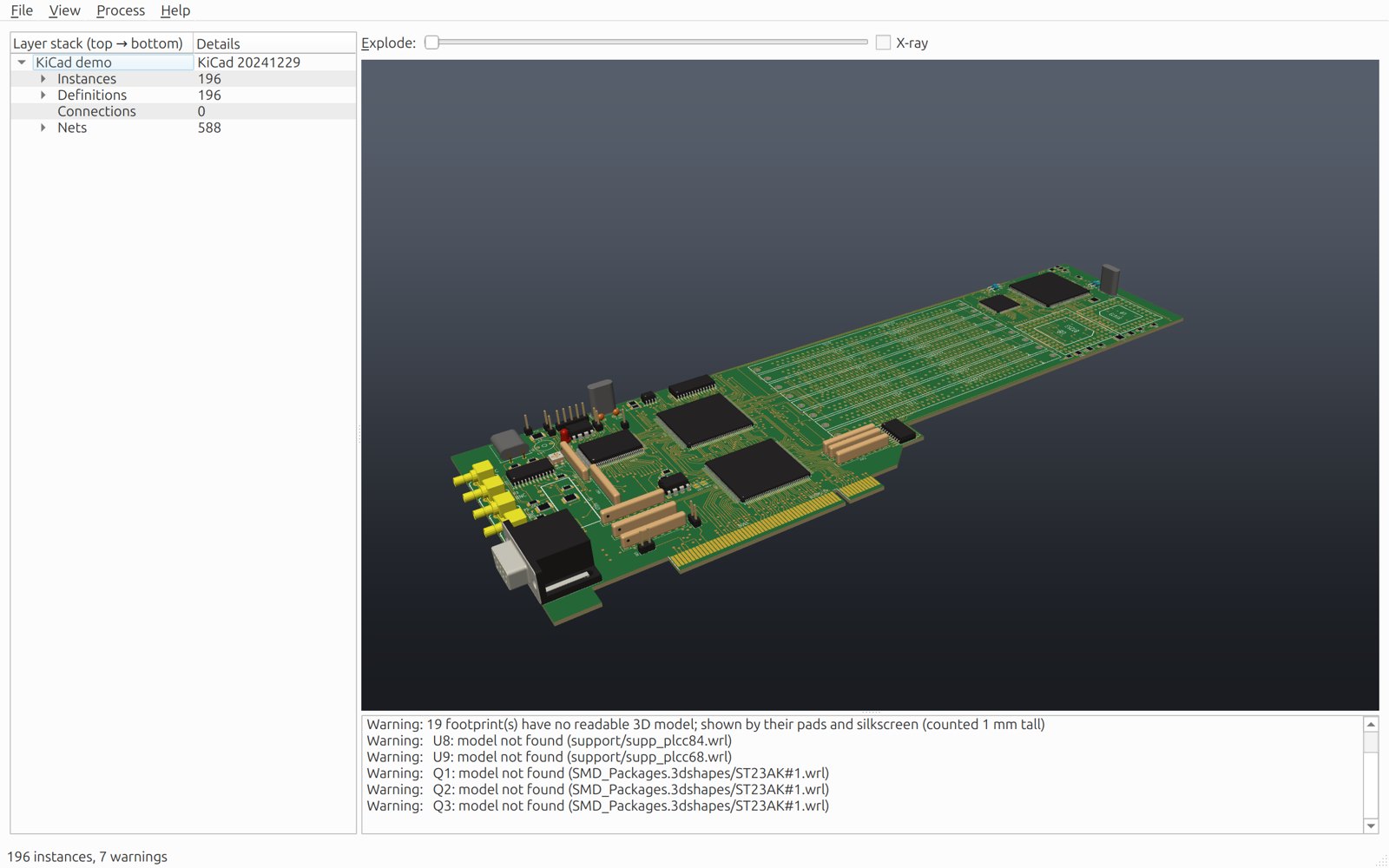
What it does today
The project is young. It can already open, show and save a complete design:
- Circuit boards from KiCad (version 6 and later): the board outline and cut-outs, every copper layer, pads, vias, the silkscreen and the board’s layer stack, with each part drawn from its own 3D model (STEP or VRML, as in KiCad).
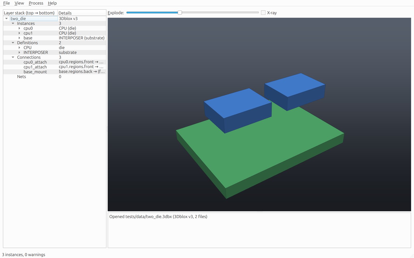
- Chiplet designs in 3Dblox, the open format for describing how chiplets are stacked and bonded, which the open-source chip tool OpenROAD also reads. Bump maps show each solder bump between the chips.
- Chip layouts in GDSII, the format chip factories take. Each metal layer is drawn at its real height above the silicon, so you can see a chip’s wiring in 3D.
- Chip, package and board together: place a chiplet design inside a part on a KiCad board, and the program adds a package under it with solder balls made from that part’s pads. Then you can follow a signal from a pad on the board up into the chips.
- Nets: click any copper, pad or bump and its whole net lights up through every layer, with the parts it touches listed.
- Exploded view and X-ray: a slider pulls the stack apart level by level, and X-ray makes the parts see-through, so nothing stays hidden inside.
- How it is built: materials, bonding methods (solder reflow, thermo-compression, hybrid bonding and others), underfill, mold and thermal paste, described in the terms of JEDEC’s JEP30 part models and drawn in place.
- Saving in open formats: designs are saved as standard 3Dblox, plus one small extra file for what 3Dblox cannot hold. We check the saved files with OpenROAD’s own 3Dblox readers, so other tools can open them.
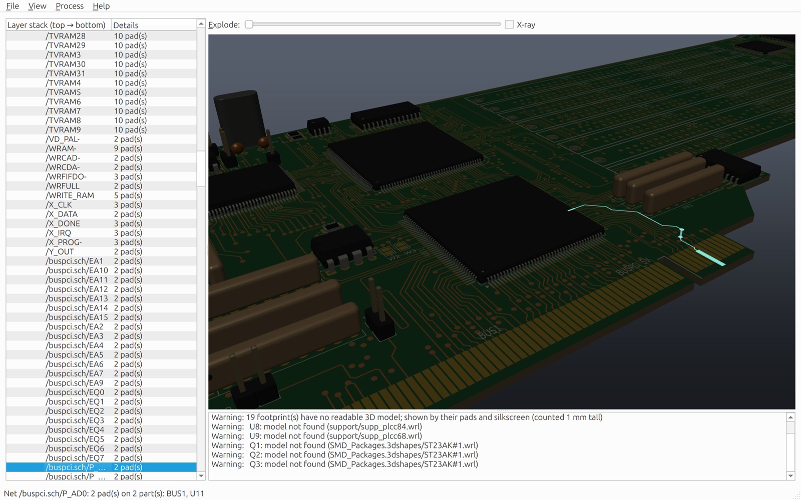
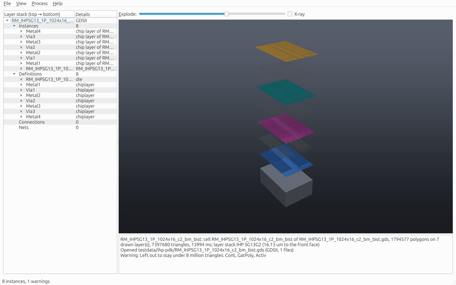
Big layouts open quickly. The SRAM above, with 1.8 million shapes, appears in under a second; what you look at sharpens over the next few seconds, the way an online map fills in as you zoom, and is kept on disk so it opens even faster next time. (It used to take 14 seconds.) The mouse wheel zooms toward whatever is under the cursor, and every view change glides smoothly instead of jumping.
Walk through a chip
Press W and you are inside the chip. You stand in one of its metal layers, between the wires, which rise around you like the walls of a building. The gaps between them become hallways. The program guides you as you walk: it keeps you in the middle of the hallway, turns with it, stops you short of a wall, and takes you into the next side hallway when you press an arrow key.
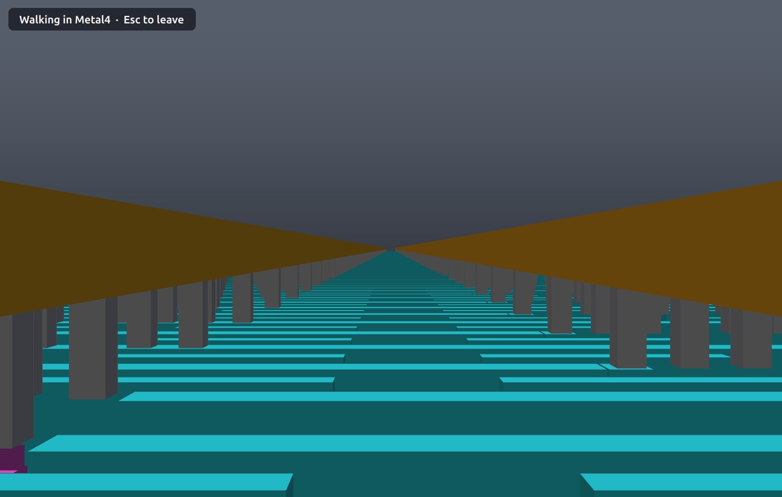
- Page Up / Page Down work like an elevator, one floor up or down. The floors are the chip’s via layers: rows of pillars that stand on one layer of wires and hold up the next, with a label showing which floor you are on.
- Space bursts through the wall straight ahead into the next hallway.
- A click with the mouse wheel on any shape, from outside or from inside, puts you on top of it: you can climb onto a wall and walk along it.
- A label shows which layer you are in, and Esc glides you back out to where you were.
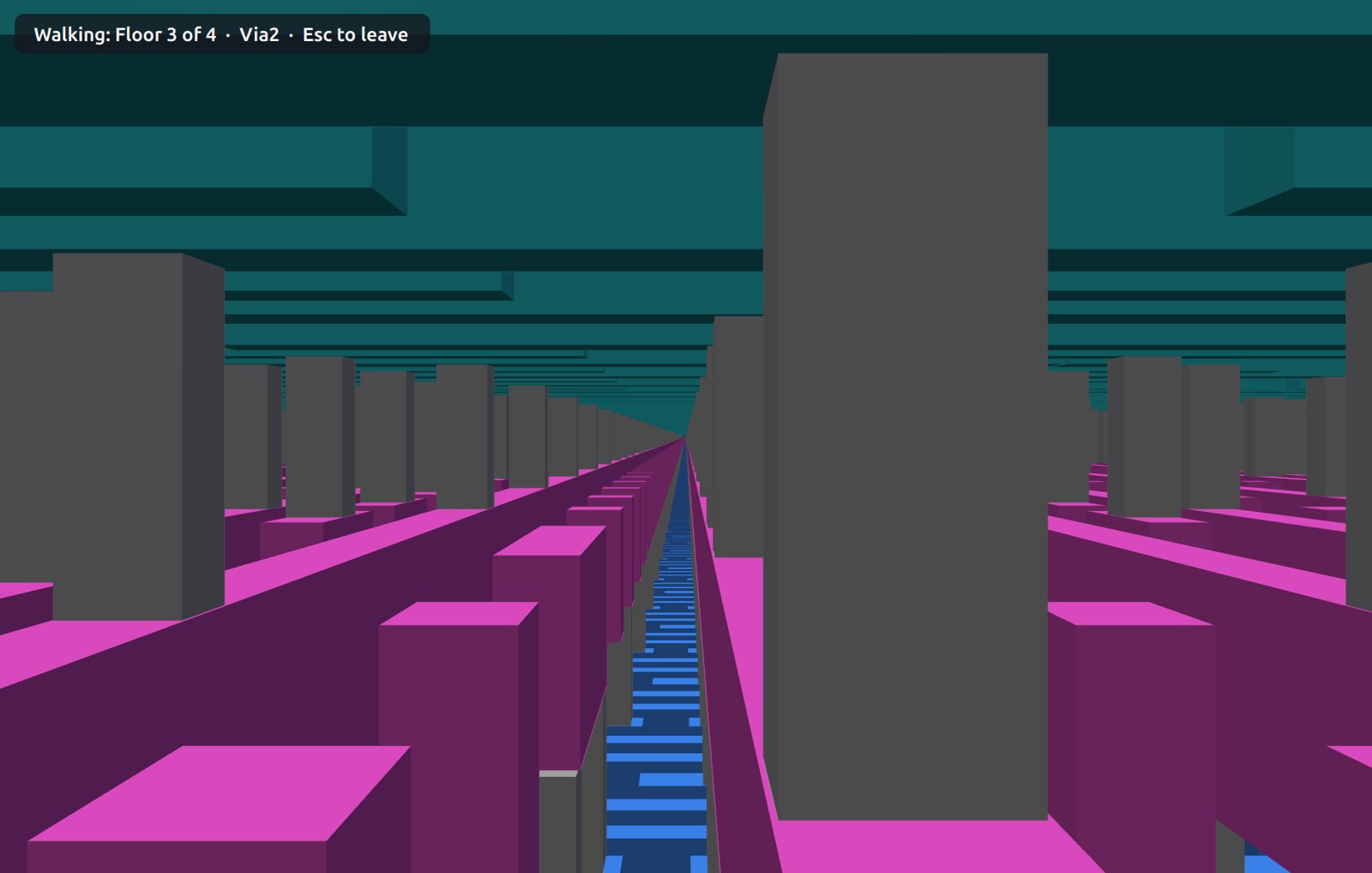
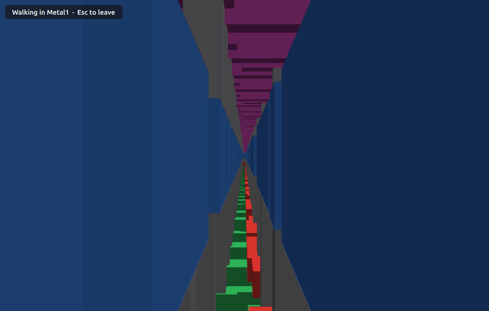
We find it the clearest way yet to understand how a chip is wired, and to show someone who has never seen the inside of one.
Open formats, so designs never get locked in
A design you make in Open PCB & IC Engineer belongs to you, not to us. It reads and writes the formats the rest of the industry uses, and it keeps its own additions in a separate file, so a strict 3Dblox reader never meets anything it does not know. KiCad stays the home of your board: the program reads the board from KiCad’s own file instead of copying it.
Sometimes a standard cannot yet carry what a real design needs. JEDEC’s JEP30, for example, says what underfill is made of but not where it goes. When that happens we do not invent a private format and keep it to ourselves. We write a proposal to the committee that maintains the standard. Our first one, eight additions to JEP30 for chiplet and 3D designs, is on our Standards Proposals page.
Where it is going
What exists today is the first of seven steps. The ones after it are:
- a stack editor for defining the chips, package and board and how they connect: bumps, balls and through-silicon vias;
- checks across the stack: is every connection made from chip to package to board, and do the layers line up and keep their distance?
- editing of layouts on any level, in 2D and 3D, and drawing schematics;
- driving proven engines instead of rewriting them: OpenROAD to place and route the chips, and ngspice to simulate the circuit;
- co-design: heat and signal estimates, and help deciding what belongs on which chip, in the package or on the board;
- output for manufacturing (GDS and OASIS for chips; Gerber, ODB++ and IPC-2581 for boards; STEP for mechanical design), with installers for Linux and Windows.
Free software
Open PCB & IC Engineer is free software under the GNU General Public License, version 3, from The JCArtes Foundation. It is written in C++ with Qt 6 and runs on Linux today. The source code is not public yet; we will publish it, with downloads, here on JCArtes.Org once the first version is ready to try.
Do you design chips, packages or boards, or teach people who do? We would like to hear what you need. Write to Support@JCArtes.Org.
See also our other Software projects.